Manufacturing method of high frequency module and high frequency module

Active Publication Date: 2021-02-11
MURATA MFG CO LTD
View PDF0 Cites 0 Cited by
  • Summary
  • Abstract
  • Description
  • Claims
  • Application Information

AI Technical Summary

Benefits of technology

[0007]In Patent Document 1, the surface layer conductor 107 is formed on the upper surface 101a of the wiring board 101 corresponding to the trench 104. Because the surface layer conductor 107 reflects a laser beam, the presence of the surface layer conductor can reduce damage to the wiring board 101 caused by the laser beam when the trench 104 is formed. However, although the damage is reduced, the conventional high frequency module 100 does not eliminate damage to the surface layer conductor 107 caused by the laser beam during laser processing, and therefore, the surface layer conductor 107 cannot be used as a signal wiring electrode. Therefore, the signal wiring electrode needs to be formed in a region of the upper surface 101a of the wiring board 101 other than the portion corresponding to the trench 104, or in an inner layer of the wiring board 101, and in this case, the size of the high frequency module 100 becomes large. Further, whe

Problems solved by technology

However, although the damage is reduced, the conventional high frequency module 100 does not eliminate damage to the surface layer conductor 10

Method used


Image

  • Manufacturing method of high frequency module and high frequency module
  • Manufacturing method of high frequency module and high frequency module
  • Manufacturing method of high frequency module and high frequency module

Examples


Example

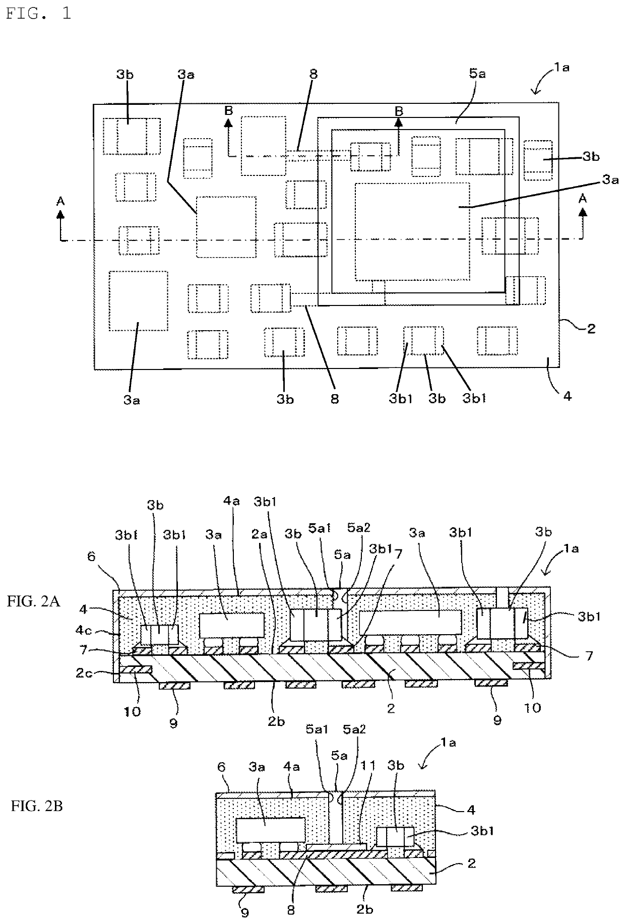
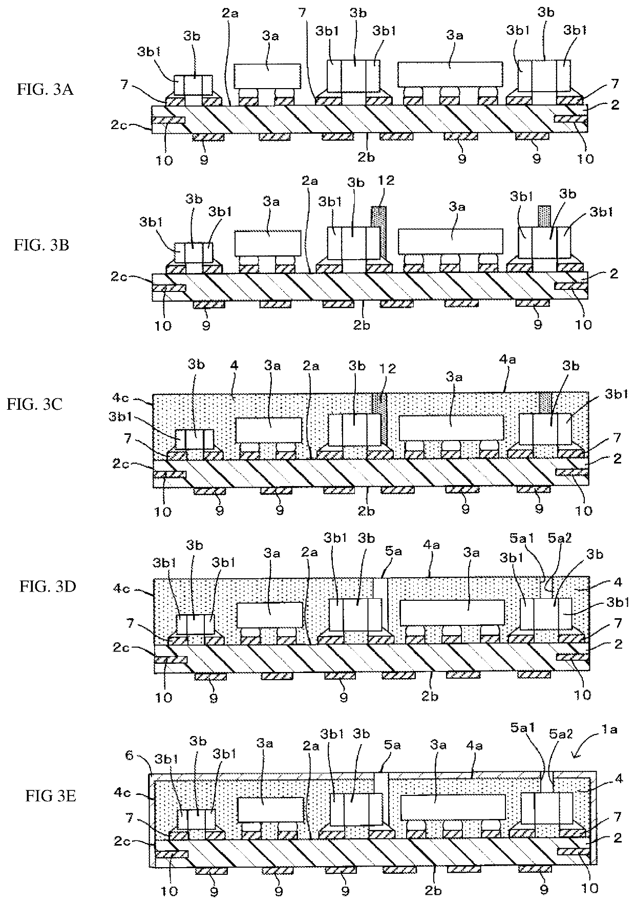
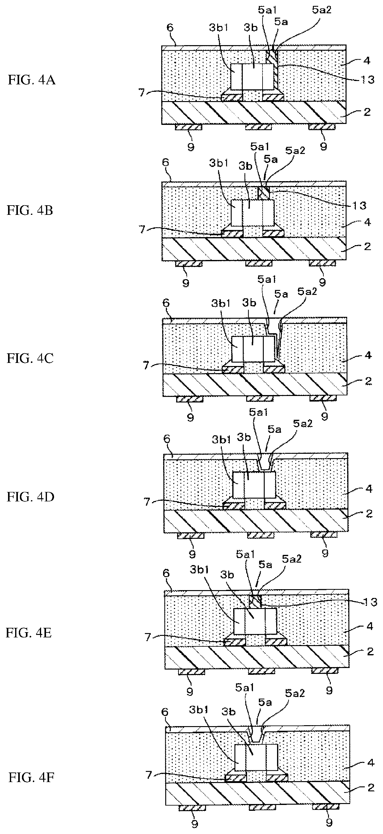
[0030]A high frequency module 1a according to a first embodiment of the present disclosure is described with reference to FIGS. 1, 2A and 2B. Note that FIG. 1 is a plan view of the high frequency module 1a with a shield film 6 removed, and FIGS. 2A and 2B are sectional views of the high frequency module 1a, in which FIG. 2A is the sectional view taken along line A-A of FIG. 1, and FIG. 2B is the sectional view taken along line B-B of FIG. 1.

[0031]As shown in FIGS. 1, 2A and 2B, the high frequency module 1a according to this embodiment includes a wiring board 2, a plurality of components 3a, 3b mounted on an upper surface 2a of the wiring board 2, a sealing resin layer 4 laminated on the upper surface 2a of the wiring board 2, a shield film 6 coating a surface of the sealing resin layer 4, and a groove 5a provided in the sealing resin layer 4, and, for example, is mounted on a mother board of an electronic instrument and the like that uses a high frequency signal.

[0032]The wiring boa...

Example

Second Embodiment

[0071]A high frequency module 1b according to a second embodiment of the present disclosure is described with reference to FIG. 6. Note that FIG. 6 is a plan view of the high frequency module 1b with a shield film 6 removed, and corresponds to FIG. 1.

[0072]The high frequency module 1b according to this embodiment is different from the high frequency module 1a of the first embodiment described with reference to FIGS. 1, 2A and 2B in, as shown in FIG. 6, the configuration of the shield groove. Other configurations are the same as those of the high frequency module 1a according to the first embodiment, and therefore, the same reference numerals are given and the descriptions thereof are omitted.

[0073]In this case, a groove 5b is formed so as to divide a sealing resin layer 4 into a plurality of regions (see FIG. 6). Specifically, when viewed from the direction perpendicular to an upper surface 2a of a wiring board 2, the groove 5b is constituted of a substantially line...

Example

Third Embodiment

[0075]A high frequency module 1c according to a third embodiment of the present disclosure is described with reference to FIG. 7. Note that FIG. 7 is a sectional view of the high frequency module 1c and corresponds to FIG. 2A.

[0076]The high frequency module 1c of this embodiment is different from the high frequency module 1a of the first embodiment described with reference to FIGS. 1, 2A and 2B in the configuration on the side of a lower surface 2b of a wiring board 2 as shown in FIG. 7. Other configurations are the same as those of the high frequency module 1a according to the first embodiment, and therefore, the same reference numerals are given and the descriptions thereof are omitted.

[0077]In this case, a plurality of mounting electrodes 70 are formed on the lower surface 2b of the wiring board 2 instead of the external electrodes 9 of the first embodiment. Further, components 3c and external terminals 14 are each mounted on the mounting electrode 70, and are sea...


PUM


Abstract

A high frequency module having a groove for shielding formed in a sealing resin layer achieves downsizing without damaging wiring electrodes formed on a wiring board or mounting components. A manufacturing method of a high frequency module includes mounting components on an upper surface of a wiring board, and then forming a sacrificial layer for forming a groove. The method further includes forming a sealing resin layer for sealing the components and the sacrificial layer, and dissolving and removing the sacrificial layer to form the groove for shielding. Finally, the method includes forming a shield film coating the surface of the sealing resin layer, and the high frequency module is manufactured. With this method, even when the groove is formed at a position overlapping with the component or a surface layer wiring electrode, the high frequency module can be downsized without damaging the component or the surface layer wiring electrode.

Description

CROSS REFERENCE TO RELATED APPLICATION[0001]This is a continuation of International Application No. PCT / JP2019 / 018206 filed on May 7, 2019 which claims priority from Japanese Patent Application No. 2018-089684 filed on May 8, 2018. The contents of these applications are incorporated herein by reference in their entireties.BACKGROUND OF THE DISCLOSUREField of the Disclosure[0002]The present disclosure relates to a high frequency module having a groove for shielding formed in a sealing resin layer and a manufacturing method thereof.Description of the Related Art[0003]A high frequency module mounted on a mobile terminal device and the like may be provided with a shield layer for shielding electromagnetic waves. In some high frequency modules of this type, there are ones in which components mounted on a wiring board are coated with a resin layer, and a shield layer is provided so as to coat the surface of the resin layer.[0004]The shield layer as such is provided to shield noise from th...

Claims


Application Information

Patent Timeline
IPC IPC(8): H01L23/552H01L21/56H01L23/66H01L23/31
CPCH01L23/552H01L23/3142H01L23/66H01L21/56H05K9/00H05K3/28H01L2924/181H01L2224/16225H01L2924/19105H01L23/3121H01L21/561H01L2924/00012
Inventor NOMURA, TADASHIKOMATSU, TORU
Owner MURATA MFG CO LTD
Why Eureka
Try Eureka