Thin film transistor panel and fabricating method thereof

Active Publication Date: 2011-11-10
SAMSUNG DISPLAY CO LTD
View PDF3 Cites 35 Cited by
  • Summary
  • Abstract
  • Description
  • Claims
  • Application Information

AI Technical Summary

Benefits of technology

[0008]An exemplary embodiment of the present invention provides a thin film tra

Problems solved by technology

In the event a TFT is fabricated using an oxide semiconductor layer, the oxide semiconductor

Method used


Image

  • Thin film transistor panel and fabricating method thereof
  • Thin film transistor panel and fabricating method thereof
  • Thin film transistor panel and fabricating method thereof

Examples


Embodiment Construction

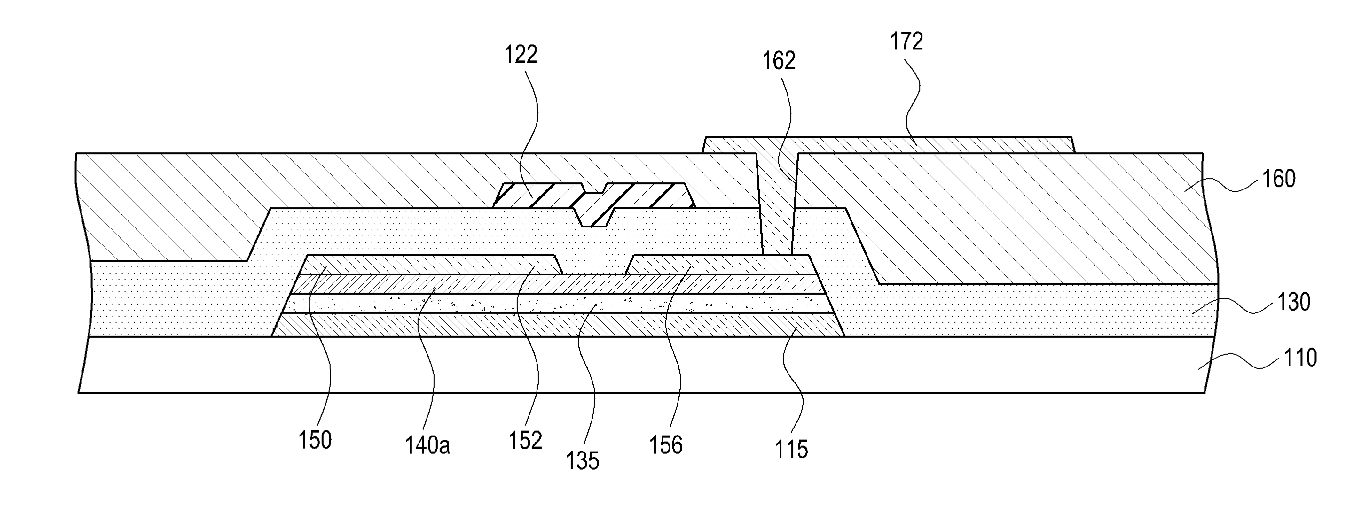
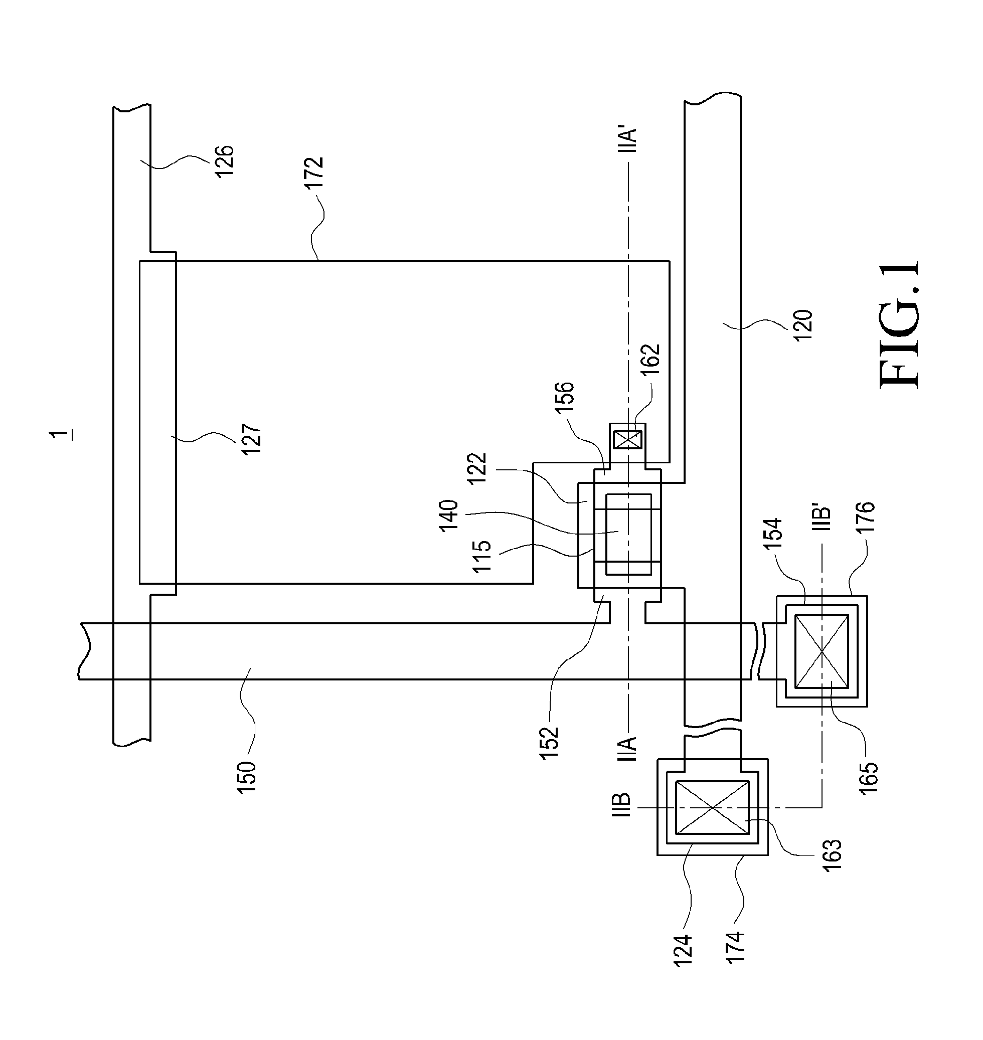
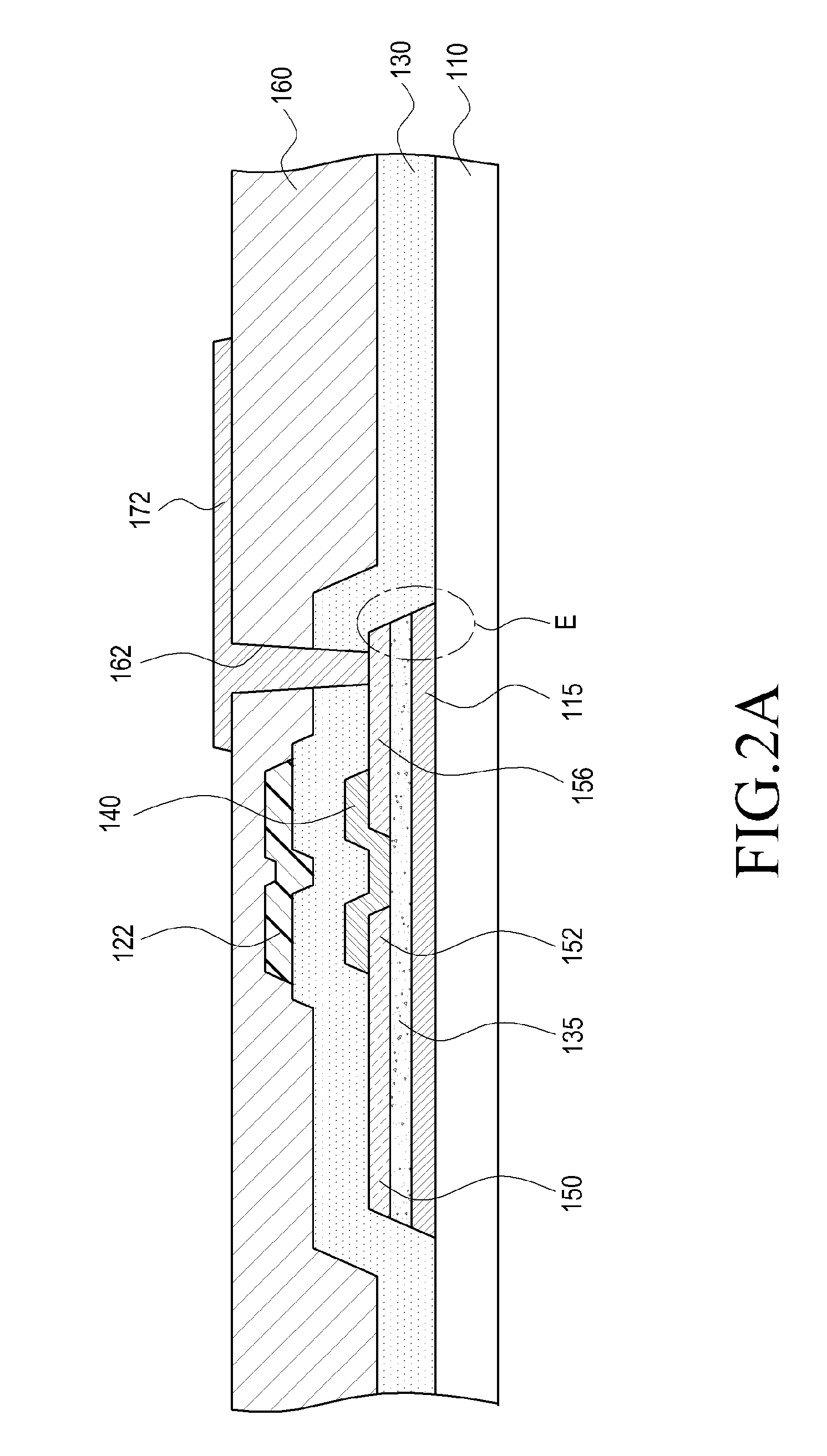
[0039]Exemplary embodiments of the present invention now will be described more fully hereinafter with reference to the accompanying drawings. The exemplary embodiments of the present invention provide various numerals of thickness and size, however, it will be understood that the scope of this invention should not be limited by them without claiming them. Also, like reference numerals refer to like elements throughout.

[0040]It will be understood that when an element or layer is referred to as being “on” or “connected to” another element or layer, it can be directly on or directly connected to the other element or layer, or intervening elements or layers may be present. In contrast, when an element is referred to as being “directly on” or “directly connected to” another element or layer, there are no intervening elements or layers present.

[0041]It will be understood that when at least two elements or layers are referred to as being “disposed along substantially the same line” or “ar...


PUM


Abstract

A thin film transistor panel includes a substrate, a light blocking layer on the substrate, a first protective film on the light blocking layer, a first electrode and a second electrode on the first protective film, an oxide semiconductor layer on a portion of the first protective film exposed between the first electrode and the second electrode, an insulating layer, a third electrode overlapping with the oxide semiconductor layer and on the insulating layer, and a fourth electrode on the insulating layer. The light blocking layer includes first sidewalls, and the first protective film includes second sidewalls. The first and the second sidewalls are disposed along substantially the same line.

Description

[0001]This application claims priority under 35 U.S.C. §119(a) to Korean Patent Application No. 10-2010-0043212, filed on May 7, 2010, the disclosure of which is incorporated by reference herein in its entirety.BACKGROUND[0002]1. Technical Field[0003]The invention relate to a thin film transistor, a thin film transistor panel and a fabricating method thereof.[0004]2. Discussion of the Related Art[0005]A flat panel display, such as a liquid crystal display (“LCD”) or an organic light emitting display (“OLED”), typically includes a plurality of pixels. The pixels are arranged in a matrix on an insulating substrate such as glass or plastic. Each pixel includes pairs of field generating electrodes and an electro-optical active layer, such as liquid crystal molecules or a light emitting layer, interposed between each pair of field generating electrodes.[0006]A pixel electrode, which is one of the electrodes in the pair of field generating electrodes, can be connected to a switching eleme...

Claims


Application Information

Patent Timeline
IPC IPC(8): H01L29/786H01L33/08H01L21/44
CPCH01L27/1225H01L27/3272H01L51/5253H01L27/1214H01L27/1288H01L27/1248H01L2227/323H10K59/126H10K59/1201H10K59/873H01L27/1218H10K50/844
Inventor RYU, HYE-YOUNGLEE, JIN-WONLEE, WOO-GEUNBYEON, HEE-JUNZHU, XUN
Owner SAMSUNG DISPLAY CO LTD
Why Eureka
Try Eureka