Compound, Light-Emitting Device, Light-Emitting Apparatus, Electronic Device, and Lighting Device

a technology of electronic devices and light-emitting devices, which is applied in the direction of luminescent compositions, chemistry apparatus and processes, and organic chemistry, can solve the problems of reducing emission efficiency and increasing the concentration ratio of guest materials, and achieve the effect of preventing energy transfer due to the dexter mechanism

Pending Publication Date: 2021-03-04
SEMICON ENERGY LAB CO LTD
View PDF8 Cites 2 Cited by
  • Summary
  • Abstract
  • Description
  • Claims
  • Application Information

AI Technical Summary

Benefits of technology

[0007]One embodiment of the present invention provides a novel compound. One embodiment of the present invention provides a novel compound that efficiently receives energy from a singlet excited state (S*) (hereinafter the energy is referred to as a singlet excitation energy) of a host material even when the concentration ratio of the guest material in an EL layer of a light-emitting device is increased, whereby the transfer of energy from a triplet excited state (T*) (the energy is hereinafter referred to as a triplet excitation energy) of the host material is unlikely to occur (energy transfer due to the Dexter mechanism can be prevented).

Problems solved by technology

As for energy transfer from a host material to a guest material in a light-emitting layer of a light-emitting device, in general it is preferable that the concentration ratio of the guest material (fluorescent substance) to the host material be increased in order to increase the efficiency of energy transfer due to the Förster mechanism; however, it is known that there is a trade-off relationship: an increase in the concentration ratio of the guest material increases the rate of energy transfer due to the Dexter mechanism, which results in a decrease in the emission efficiency.
Therefore, increasing the concentration ratio of the guest material has not been an effective means for improving the emission efficiency.

Method used


Image

  • Compound, Light-Emitting Device, Light-Emitting Apparatus, Electronic Device, and Lighting Device
  • Compound, Light-Emitting Device, Light-Emitting Apparatus, Electronic Device, and Lighting Device
  • Compound, Light-Emitting Device, Light-Emitting Apparatus, Electronic Device, and Lighting Device

Examples


embodiment 1

[0108]In this embodiment, compounds that are embodiments of the present invention will be described. A compound of one embodiment of the present invention is represented by General Formula (G1) below.

[0109]In General Formula (G1), A represents a substituted or unsubstituted condensed aromatic ring having 10 to 30 carbon atoms or a substituted or unsubstituted condensed heteroaromatic ring having 10 to 30 carbon atoms, and R1 represents a substituted or unsubstituted aryl group having 6 to 25 carbon atoms. Each of Y1 and Y2 independently represents a cycloalkyl group having a bridge structure and having 7 to 10 carbon atoms.

[0110]In another embodiment of the present invention, in General Formula (G1), R1 represents an aryl group having 6 to 25 carbon atoms, the aryl group includes two or more substituents, and each of the two or more substituents independently represents any one of an alkyl group having 3 to 10 carbon atoms, a substituted or unsubstituted cycloalkyl group having 3 to...

embodiment 2

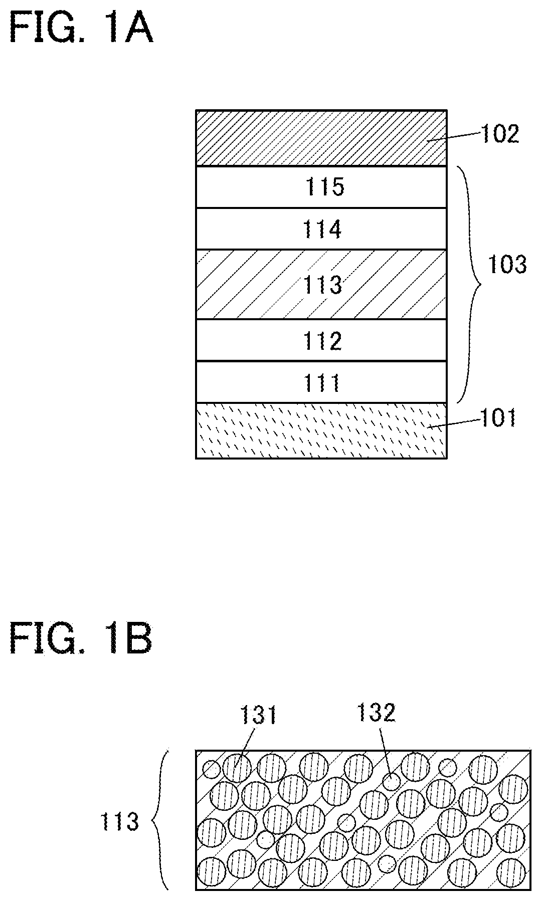
[0153]In this embodiment, examples of light-emitting devices for which a compound of one embodiment of the present invention is preferably used will be described. As illustrated in FIG. 1A, the light-emitting device has a structure in which an EL layer 103 is positioned between a pair of electrodes, a first electrode 101 (corresponding to an anode in FIG. 1A) and a second electrode 102 (corresponding to a cathode in FIG. 1A). The EL layer 103 includes at least a light-emitting layer 113. In addition, functional layers, such as a hole-injection layer III, a hole-transport layer 112, an electron-transport layer 114, and an electron-injection layer 115, can be provided.

[0154]The light-emitting layer 113 contains a light-emitting substance (a guest material) and a host material. In the light-emitting device, voltage application between the pair of electrodes causes injection of electrons and holes from the cathode and the anode, respectively, into the EL layer 103; thus, current flows. ...

embodiment 3

[0252]In this embodiment, light-emitting devices of embodiments of the present invention will be described.

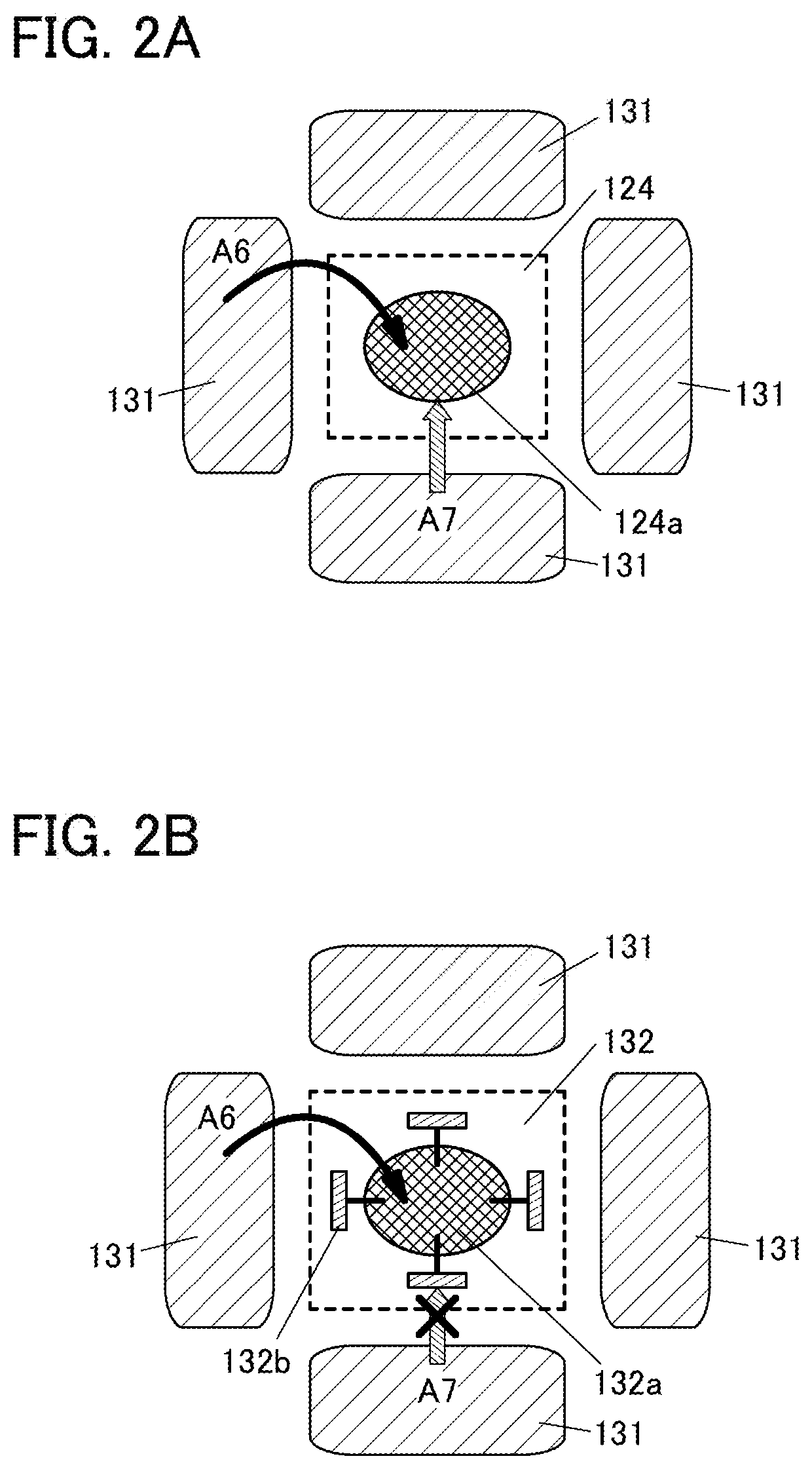
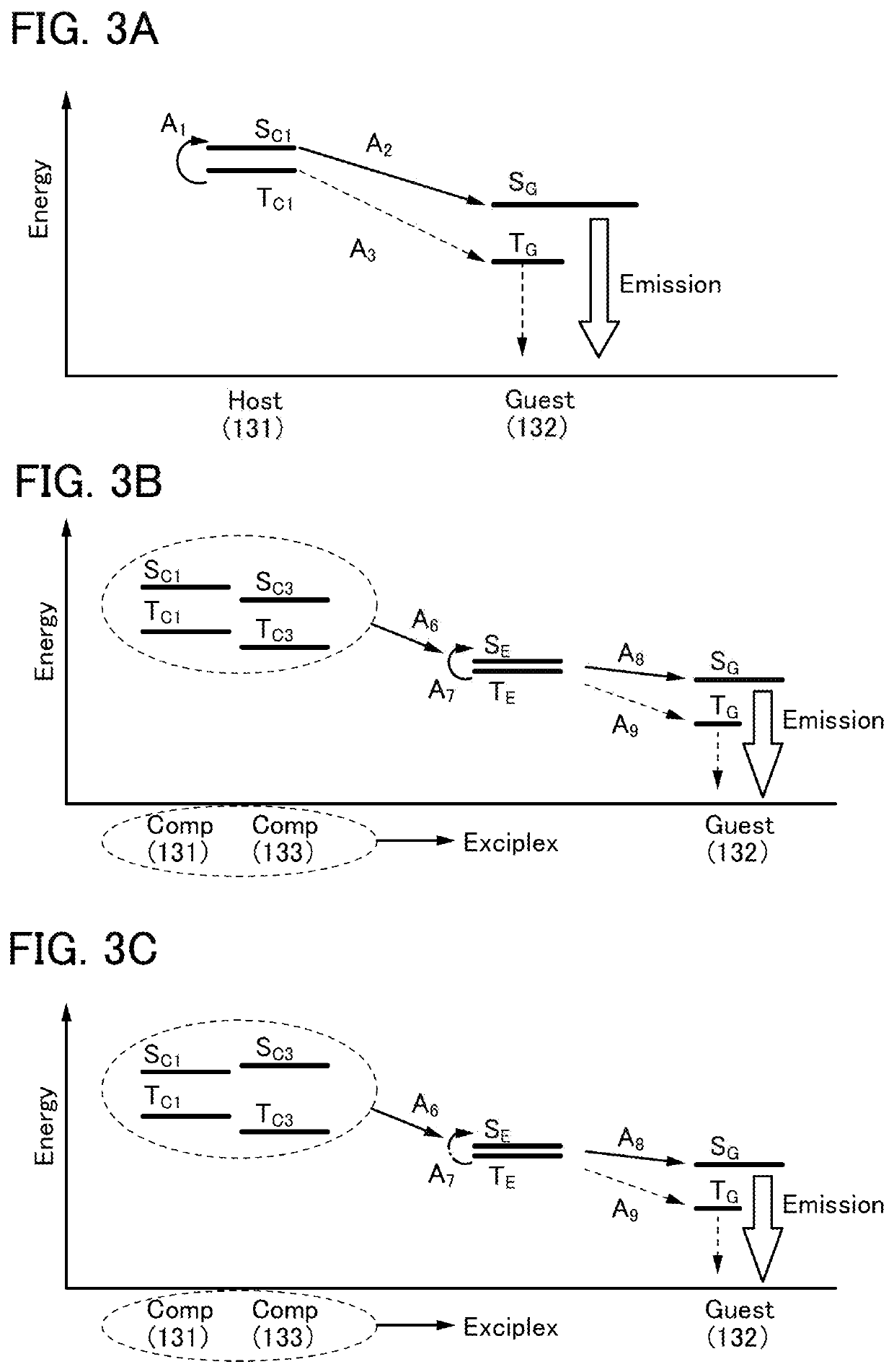
[0253]FIG. 6A illustrates an example of a light-emitting device including an EL layer that includes a light-emitting layer between a pair of electrodes. Specifically, an EL layer 103 is provided between a first electrode 101 and a second electrode 102. For example, in the case where the first electrode 101 is an anode, the EL layer 103 has a structure in which a hole-injection layer 111, a hole-transport layer 112, a light-emitting layer 113, an electron-transport layer 114, and an electron-injection layer 115 are stacked as functional layers in this order. The light-emitting layer 113 includes a host material and guest materials. A third organic compound 123 is used as the host material, and a first organic compound 121 (fluorescent substance) that has a function of converting singlet excitation energy into light emission and a second organic compound 122 (phosphorescent subst...


PUM

PropertyMeasurementUnit
distanceaaaaaaaaaa
visible light transmittanceaaaaaaaaaa
visible light reflectanceaaaaaaaaaa

Abstract

A novel compound is provided. The novel compound is represented by General Formula (G1).
In General Formula (G1), A represents a substituted or unsubstituted condensed aromatic ring having 10 to 30 carbon atoms or a substituted or unsubstituted condensed heteroaromatic ring having 10 to 30 carbon atoms, and R1 represents a substituted or unsubstituted aryl group having 6 to 25 carbon atoms. Each of Y1 and Y2 independently represents a cycloalkyl group having a bridge structure and having 7 to 10 carbon atoms.

Description

BACKGROUND OF THE INVENTION1. Field of the Invention[0001]One embodiment of the present invention relates to a compound, a light-emitting device, a light-emitting apparatus, an electronic device, and a lighting device. Note that one embodiment of the present invention is not limited thereto. That is, one embodiment of the present invention relates to an object, a method, a manufacturing method, or a driving method. One embodiment of the present invention relates to a process, a machine, manufacture, or a composition of matter.2. Description of the Related Art[0002]In recent years, research and development of light-emitting devices using electroluminescence (EL) have been actively conducted. Such a light-emitting device has a structure in which an EL layer (containing a light-emitting substance) is provided between a pair of electrodes. In a light-emitting device, voltage application between the pair of electrodes causes, in the EL layer, recombination of electrons and holes injected...

Claims


Application Information

Patent Timeline
Patent Type & Authority Applications(United States)
IPC IPC(8): H01L51/00C09K11/02C09K11/06C07C211/61
CPCH01L51/006C09K11/02C09K11/06H01L51/5016C09K2211/185C09K2211/1007C09K2211/1044C07C211/61C07C2603/24C07C2603/74C07C2602/42C07C2603/68C09K2211/1011C09K2211/1014H10K85/626H10K85/633H10K85/615H10K50/11C07C2603/50C07C2603/94C07C2601/14H10K59/12H10K85/622H10K85/654H10K85/342H10K85/6572H10K50/19H10K2102/3026H10K2101/27H10K2101/90C07C211/54C07C211/57H10K85/621H10K71/00H10K50/121H10K50/858H10K50/8426H10K59/38H10K59/131H10K59/351H10K2101/10H10K2102/3035
Inventor HARUYAMA, TAKUYASEO, SATOSHIOHSAWA, NOBUHARU
Owner SEMICON ENERGY LAB CO LTD
Why Eureka
Try Eureka