Liquid crystal panel and manufacturing method thereof
a technology of liquid crystal panels and manufacturing methods, applied in non-linear optics, instruments, optics, etc., can solve the problem of reducing the screen-to-body ratio of products, and achieve the effect of reducing the problem of excessive frame width
- Summary
- Abstract
- Description
- Claims
- Application Information
AI Technical Summary
Benefits of technology
Problems solved by technology
Method used
Image
Examples
Embodiment Construction
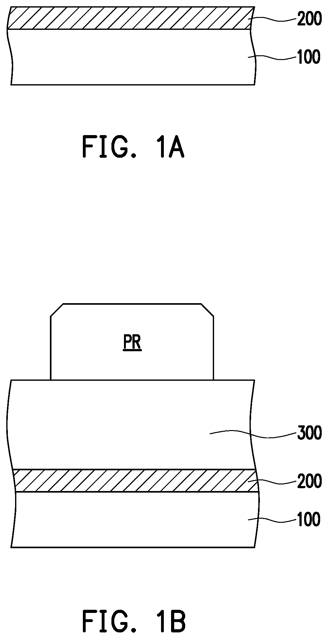
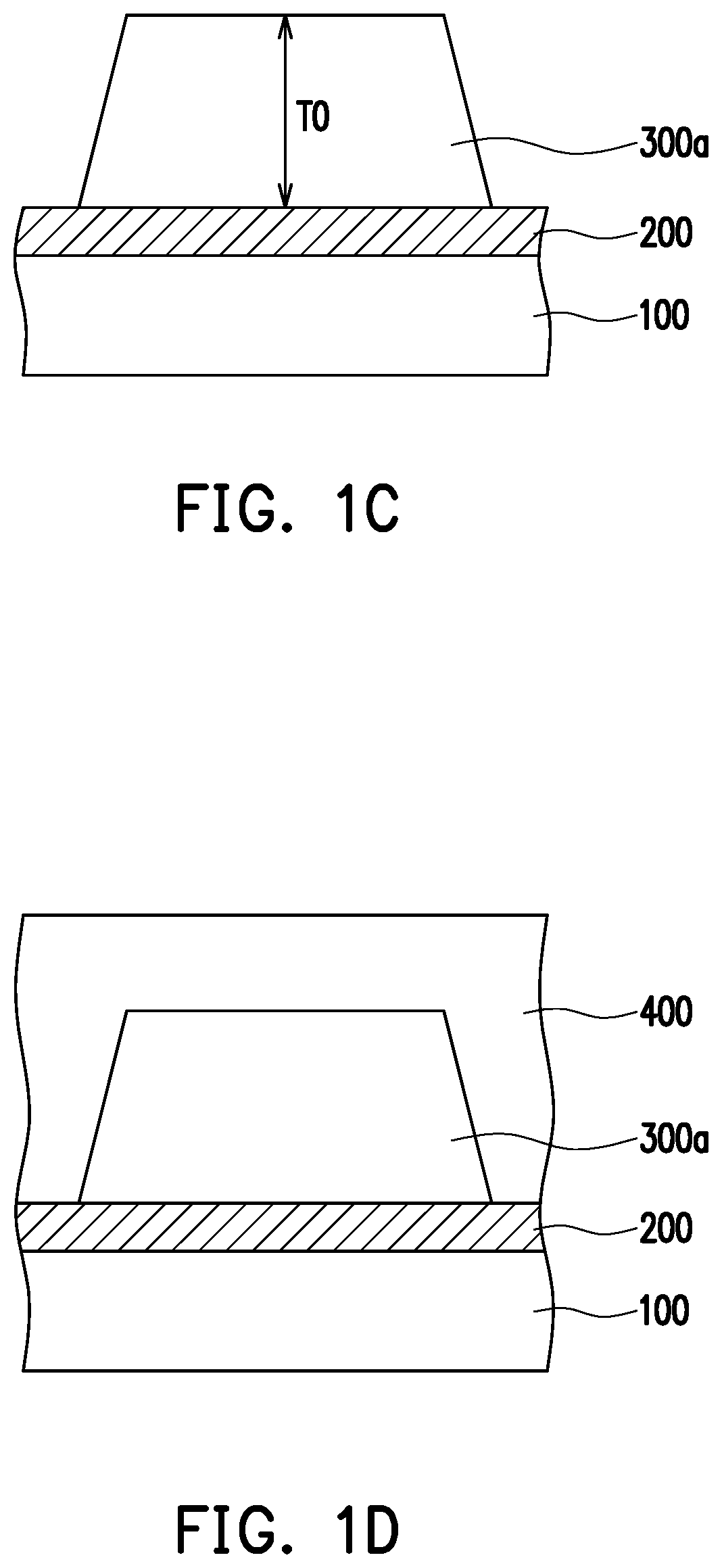
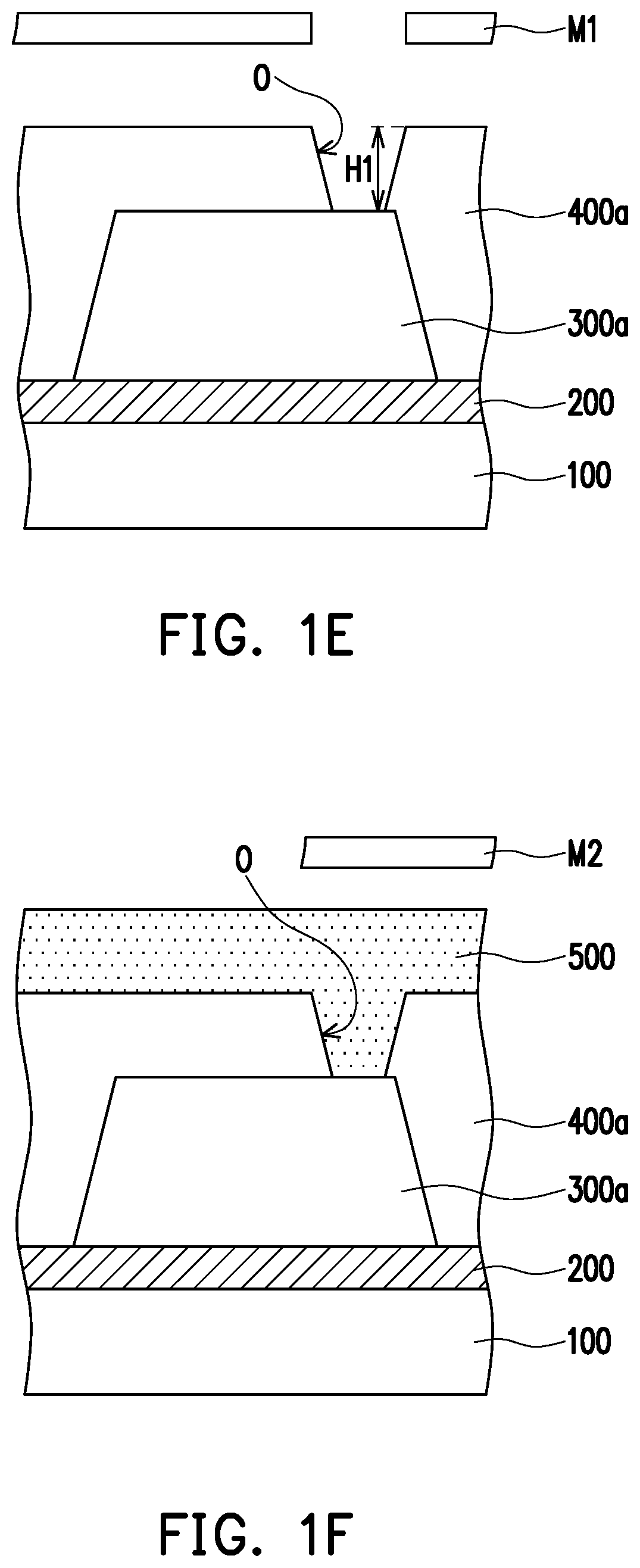
[0017]FIG. 1A to FIG. 1K are each a schematic cross-sectional view of a manufacturing method of a liquid crystal panel according to an embodiment of the invention.
[0018]Referring to FIG. 1A first, an electrode layer 200 is formed on a substrate 100. The substrate 100 is made of glass, quartz, organic polymer or other applicable materials. A thickness of the substrate 100 is, for example, hundreds of microns to several millimeters. For example, the thickness of the substrate 100 is 0.5 millimeters, but the invention is not limited thereto.
[0019]The electrode layer 200 is made of transparent conductive oxide. For example, the electrode layer 200 is made of indium tin oxide, indium zinc oxide, aluminum tin oxide, aluminum zinc oxide, indium gallium zinc oxide or a stack layer of at least two of the foregoing, but the invention is not limited thereto.
[0020]In some embodiments, other element layers are included between the electrode layer 200 and the substrate 100. Therefore, an electric...
PUM
 Abstract
Description
Claims
Application Information


