

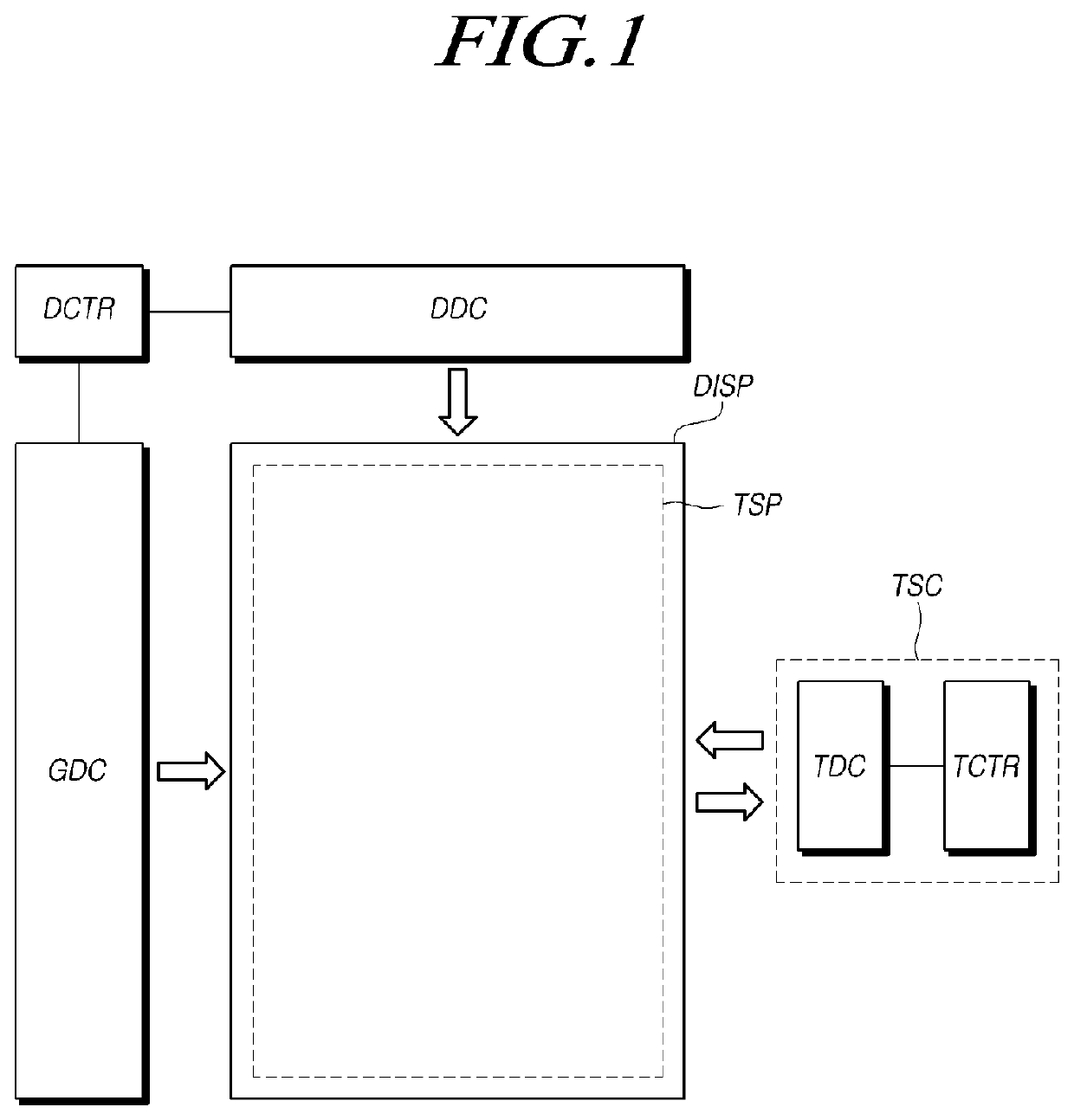
Touch Display Device
a display device and touch technology, applied in semiconductor devices, instruments, computing, etc., can solve problems such as deteriorating the performance of touch sensing, and achieve the effects of reducing parasitic capacitance, parasitic capacitance, and resistance of touch routing lines
- Summary
- Abstract
- Description
- Claims
- Application Information
AI Technical Summary
Benefits of technology
Problems solved by technology
Method used
Image

Examples
Embodiment Construction
[0034]In the following description of examples or embodiments of the disclosure, reference will be made to the accompanying drawings in which it is shown by way of illustration specific examples or embodiments that can be implemented, and in which the same reference numerals and signs can be used to designate the same or like components even when they are shown in different accompanying drawings from one another. Further, in the following description of examples or embodiments of the disclosure, detailed descriptions of well-known functions and components incorporated herein will be omitted when it is determined that the description may make the subject matter in some embodiments of the disclosure rather unclear. The terms such as “including”, “having”, “containing”, “constituting”“make up of”, and “formed of” used herein are generally intended to allow other components to be added unless the terms are used with the term “only”. As used herein, singular forms are intended to include...
PUM
 Abstract
Description
Claims
Application Information