Method of forming a structure including silicon oxide

a technology of silicon oxide and bpsg, which is applied in the direction of coating, chemical vapor deposition coating, metallic material coating process, etc., can solve the problems of bpsg generally unsuitable for filling gaps of nm-order three-dimensional patterns, voids can form within the deposited material, and cvd-deposited bpsg exhibits relatively poor step coverag

Pending Publication Date: 2021-05-13
ASM IP HLDG BV
View PDF2 Cites 136 Cited by
  • Summary
  • Abstract
  • Description
  • Claims
  • Application Information

AI Technical Summary

Benefits of technology

[0012]These and other embodiments will become readily apparent to those skilled in the art from the following detailed description of c

Problems solved by technology

For example, CVD-deposited BPSG exhibits relatively poor step coverage, and thus voids can form within the deposited material.
Further, the relatively high film growth rate of CVD-deposited BPSG makes BPSG generally unsuitable for filling gaps of nm-order three-dimensional patterns.
Additionally, under-

Method used


Image

  • Method of forming a structure including silicon oxide
  • Method of forming a structure including silicon oxide
  • Method of forming a structure including silicon oxide

Examples


Embodiment Construction

[0020]Although certain embodiments and examples are disclosed below, it will be understood by those in the art that the invention extends beyond the specifically disclosed embodiments and / or uses of the invention and obvious modifications and equivalents thereof. Thus, it is intended that the scope of the invention disclosed should not be limited by the particular disclosed embodiments described below.

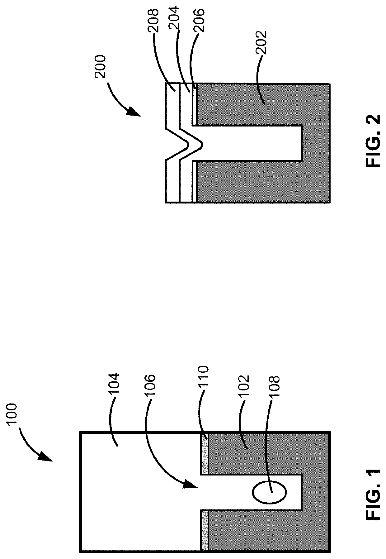
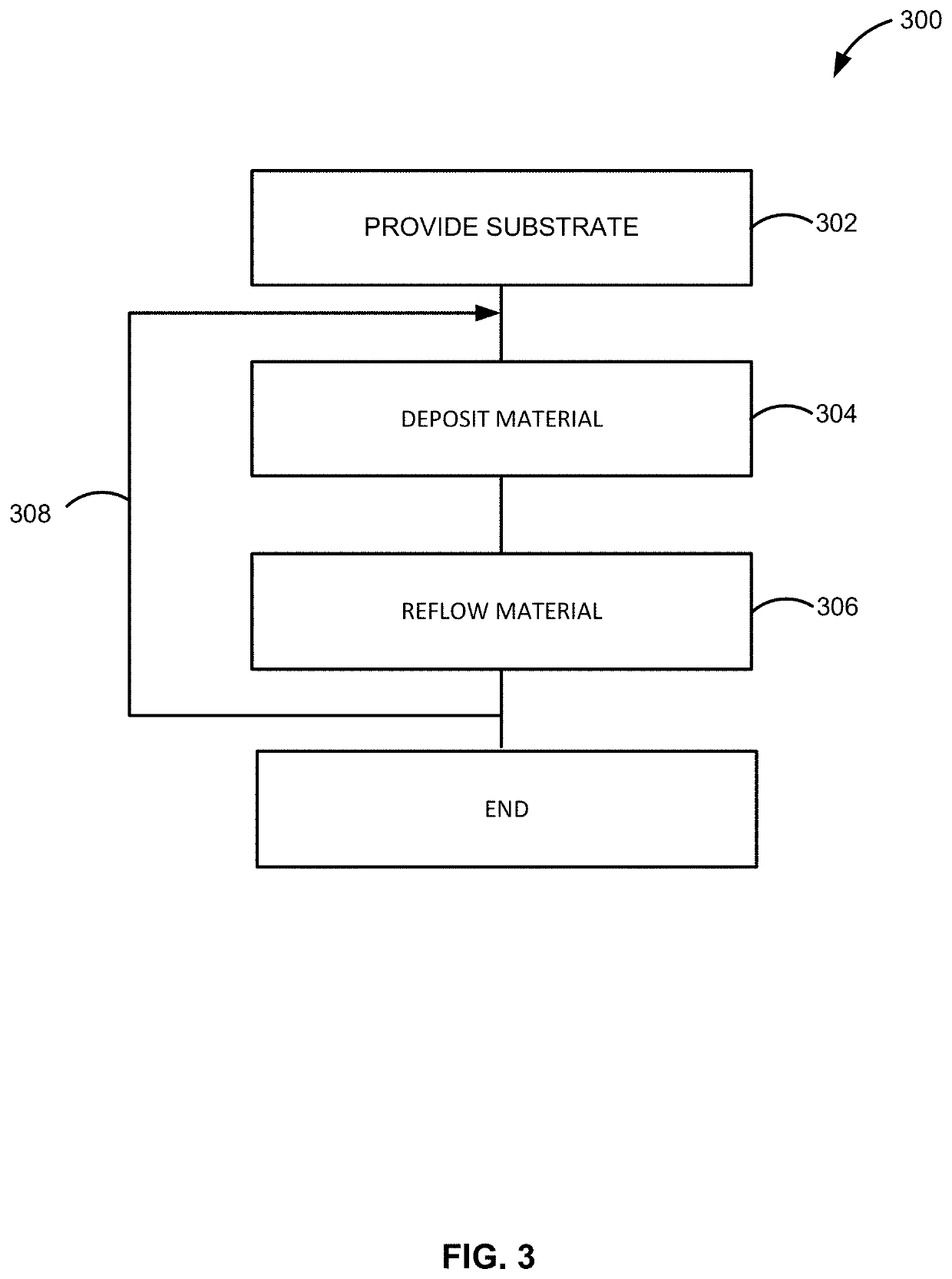
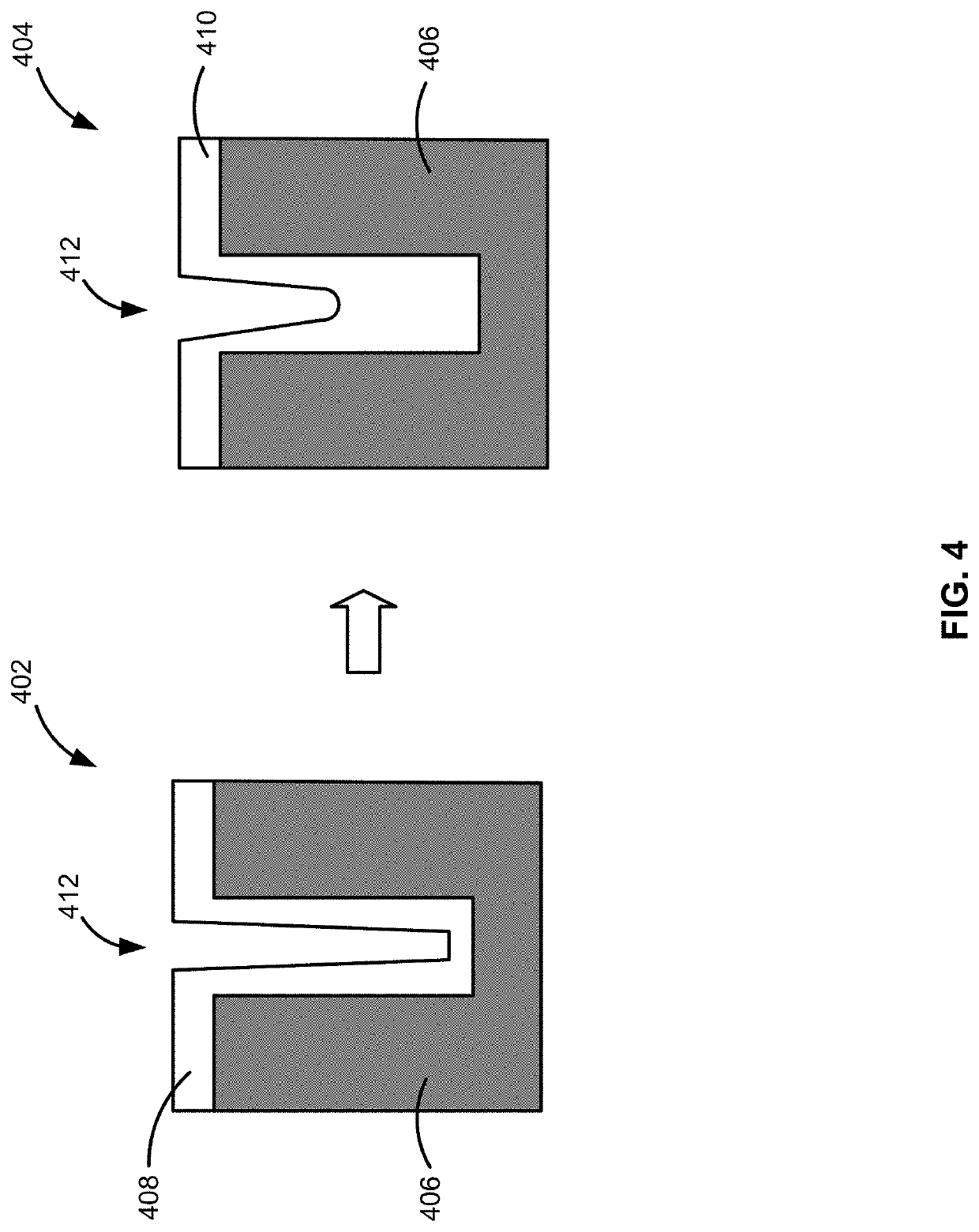
[0021]The present disclosure generally relates to methods of depositing materials, to methods of forming structures, and to structures formed using the methods. Byway of examples, the methods described herein can be used to fill features, such as gaps (e.g., trenches or vias) on a surface of a substrate with material, such as insulating (e.g., dielectric) material. By way of particular examples, a chemical formula of the material can include Si and O. As set forth in more detail below, the chemical formula can additionally include one or more (e.g., two or more, three or more, or the l...


PUM

PropertyMeasurementUnit
Temperatureaaaaaaaaaa

Abstract

Methods for depositing on a surface of a substrate are disclosed. Exemplary methods include depositing a silicon oxide material using a cyclical deposition process, and reflowing the material during one or more of the step of depositing and a post-deposition anneal step. Structures including a layer of the material are also disclosed.

Description

CROSS-REFERENCE TO RELATED APPLICATIONS[0001]This application claims the benefit of U.S. Provisional Application No. 62 / 933,693, filed on Nov. 11, 2019, in the United States Patent and Trademark Office, the disclosure of which is incorporated herein in its entirety by reference.FIELD OF INVENTION[0002]The present disclosure generally relates to methods of forming structures suitable for use in the manufacture of electronic devices. More particularly, examples of the disclosure relate to methods that include formation of silicon oxide layers.BACKGROUND OF THE DISCLOSURE[0003]During the manufacture of devices, such as semiconductor devices, it is often desirable to fill features (e.g., trenches or gaps) on the surface of a substrate with insulating or dielectric material. Some techniques to fill features include the deposition and reflow of borophosphosilicate glass (BPSG).[0004]Use of BPSG in the manufacture of electronic devices has been reported since the 1970s. BPSG films can be d...

Claims


Application Information

Patent Timeline
IPC IPC(8): H01L21/02C23C16/40C23C16/455
CPCH01L21/0228C23C16/45538C23C16/45553C23C16/401C23C16/045C23C16/0272C23C16/45531C23C16/45527C23C16/46H01L21/02164H01L21/02274H01L21/02129H01L21/02304H01L21/31051H01L21/02123H01L21/022H01L21/02208H01L21/02356C23C16/402C23C16/45536C23C16/56
Inventor FUKUDA, HIDEAKIUEDA, SHINYAKIMURA, KAZUHIRO
Owner ASM IP HLDG BV
Why Eureka
Try Eureka