Display device

a display device and display technology, applied in the field of display devices, can solve the problems of reducing the life of the electrical element included in the display device, affecting and damage to the electrical element, so as to improve the sensitivity of reduce the parasitic capacitance between the light emitting element and the input sensing layer

Active Publication Date: 2021-06-10
SAMSUNG DISPLAY CO LTD
View PDF0 Cites 1 Cited by
  • Summary
  • Abstract
  • Description
  • Claims
  • Application Information

AI Technical Summary

Benefits of technology

[0029]In the display device according to the exemplary embodiments, the encapsulation layer may include the organic encapsulation layer that includes organic material having a permittivity less than or equal to about 3.0 or hollow particles dispersed in the organic material, and the low permittivity layer including hollow particles dispersed in organic material or the organic material having a permittivity less than or equal to about 3.0 may be disposed on the encapsulation layer. Accordingly, a parasitic capacitance between the light emitting element and the input sensing layer may decrease, and sensitivity of the input sensing layer may be improved.

Problems solved by technology

The lifespan of an electrical element included in the display device may decrease when impurities such as gas, moisture or other contaminants flow into the display device from outside which may damage the electrical elements.
The light efficiency of the organic light emitting layer may also decrease when impurities flow into the organic light emitting display device.
However, when the distance between the input sensing layer and the light emitting element decreases due to a reduced thickness of the encapsulation layer, a parasitic capacitance formed between an electrode of the light emitting and a sensing electrode of the input sensing layer may increase.

Method used


Image

  • Display device
  • Display device
  • Display device

Examples


Embodiment Construction

[0040]Hereinafter, display devices in accordance with exemplary embodiments of the present inventive concepts will be explained in detail with reference to the accompanying drawings.

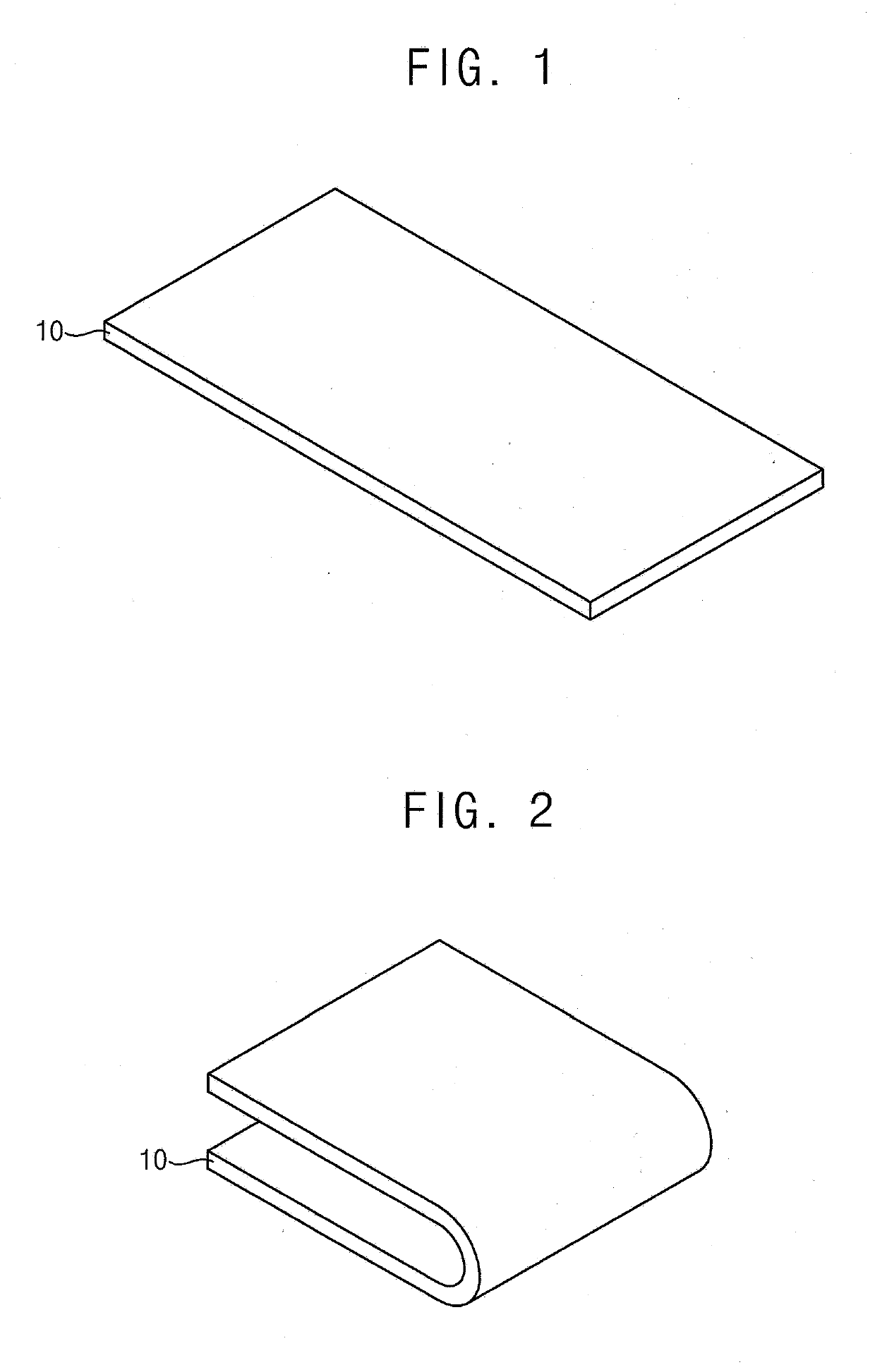
[0041]FIGS. 1 and 2 are perspective views illustrating a display device 10 in a folded state and an unfolded state, according to exemplary embodiments of the present inventive concepts.

[0042]Referring to FIGS. 1 and 2, a display device 10 according to an exemplary embodiment may be a flexible display device. For example, the display device 10 may be a foldable display device. The display device 10 may be in an unfolded state as illustrated in FIG. 1, or may be in a folded state as illustrated in FIG. 2. However, exemplary embodiments of the present inventive concepts are not limited thereto. For example, in other exemplary embodiments, the display device 10 may be a bendable display device, a rollable display device, etc. In another exemplary embodiment, the display device 10 may not be flexible.
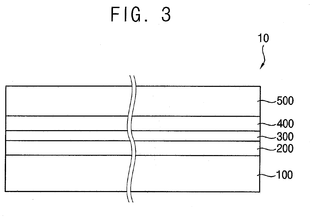
[0043]FI...


PUM

PropertyMeasurementUnit
diameteraaaaaaaaaa
thicknessaaaaaaaaaa
DAaaaaaaaaaa

Abstract

A display device may include a substrate and a light emitting element disposed on the substrate. An encapsulation layer covers the light emitting element. The encapsulation layer includes at least two inorganic encapsulation layers and at least one organic encapsulation layer. The at least one organic encapsulation layer includes a first organic material having a permittivity less than or equal to about 3.0. A low permittivity layer is disposed on the encapsulation layer. The low permittivity layer includes a second organic material and first hollow particles dispersed in the second organic material. An input sensing layer is disposed on the low permittivity layer.

Description

CROSS-REFERENCE TO RELATED APPLICATION(S)[0001]This application claims priority under 35 U.S.C. § 119 to Korean Patent Application No. 10-2019-0161694, filed on Dec. 6, 2019 in the Korean Intellectual Property Office, the disclosure of which is incorporated by reference in its entirety herein.1. TECHNICAL FIELD[0002]The present inventive concepts relate to a display device. More particularly, the present inventive concepts relate to a display device including an input sensing layer.2. DISCUSSION OF RELATED ART[0003]A display device, such as a liquid crystal display device, an organic light emitting display device, an electrophoretic display device, or the like, may include electric field generating electrodes and an electro-optical active layer formed therebetween. For example, an organic light emitting display device may include a light emitting element having an organic light emitting layer as the electro-optical active layer.[0004]The lifespan of an electrical element included in...

Claims


Application Information

Patent Timeline
Patent Type & Authority Applications(United States)
IPC IPC(8): H01L51/52H01L27/32G06F3/044G06F3/041
CPCH01L51/5253H01L27/323H01L51/5256G06F2203/04102G06F3/0446G06F3/0412H01L27/3244G06F3/0443G09F9/301H10K59/40H10K50/8445H10K50/84G06F2203/04103H10K50/858H10K50/844H10K2102/331H10K2102/00H10K2102/351H10K59/12
Inventor KIM, YI SUKIM, YOUNG GUSONG, CHANG YEONGYANG, HYE INJUNG, WOO SUKJU, YONG CHANHA, JAE HEUNG
Owner SAMSUNG DISPLAY CO LTD
Why Eureka
Try Eureka