Contactless Communication Module

a communication module and contactless technology, applied in the direction of transmission, printed circuit manufacturing, near-field systems using receivers, etc., can solve the problems of become more difficult to design the contactless communication electric circuit and the electric circuit, and achieve the effect of improving communication accuracy

Inactive Publication Date: 2021-06-17
HOSIDEN CORP
View PDF2 Cites 0 Cited by
  • Summary
  • Abstract
  • Description
  • Claims
  • Application Information

AI Technical Summary

Benefits of technology

[0009]Such contactless communication module provides improved communication accuracy. This is because the antenna is disposed at the same height position as, or on one side of the first direction relative to, the semiconductor component. This arrangement decreases the distance in the first direction from the antenna to a partner communication device disposed at a short distance from, and on the one side of the first direction relative to, the base.
[0031]The contactless communication module according to any of the above aspects may further include a second conductor. The second conductor may be disposed on one side of the first direction relative to the antenna and grounded. The second conductor may have an opening located on one side of the first direction relative to at least a part of the antenna. Such contactless communication module provides further improved communication accuracy.

Problems solved by technology

In particular, it is more difficult to design the communication electric circuit as the communication speed of contactless communication increases.
For this reason, it has become more difficult to design the electric circuit for contactless communication and the electric circuit for main functions of an electronic device on the same circuit board of the electronic device.

Method used


Image

  • Contactless Communication Module
  • Contactless Communication Module
  • Contactless Communication Module

Examples


first embodiment

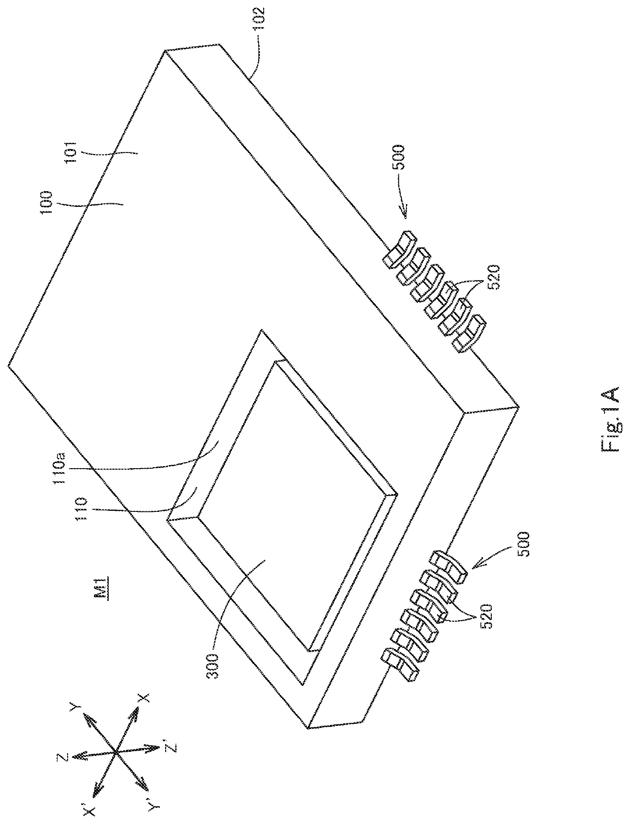
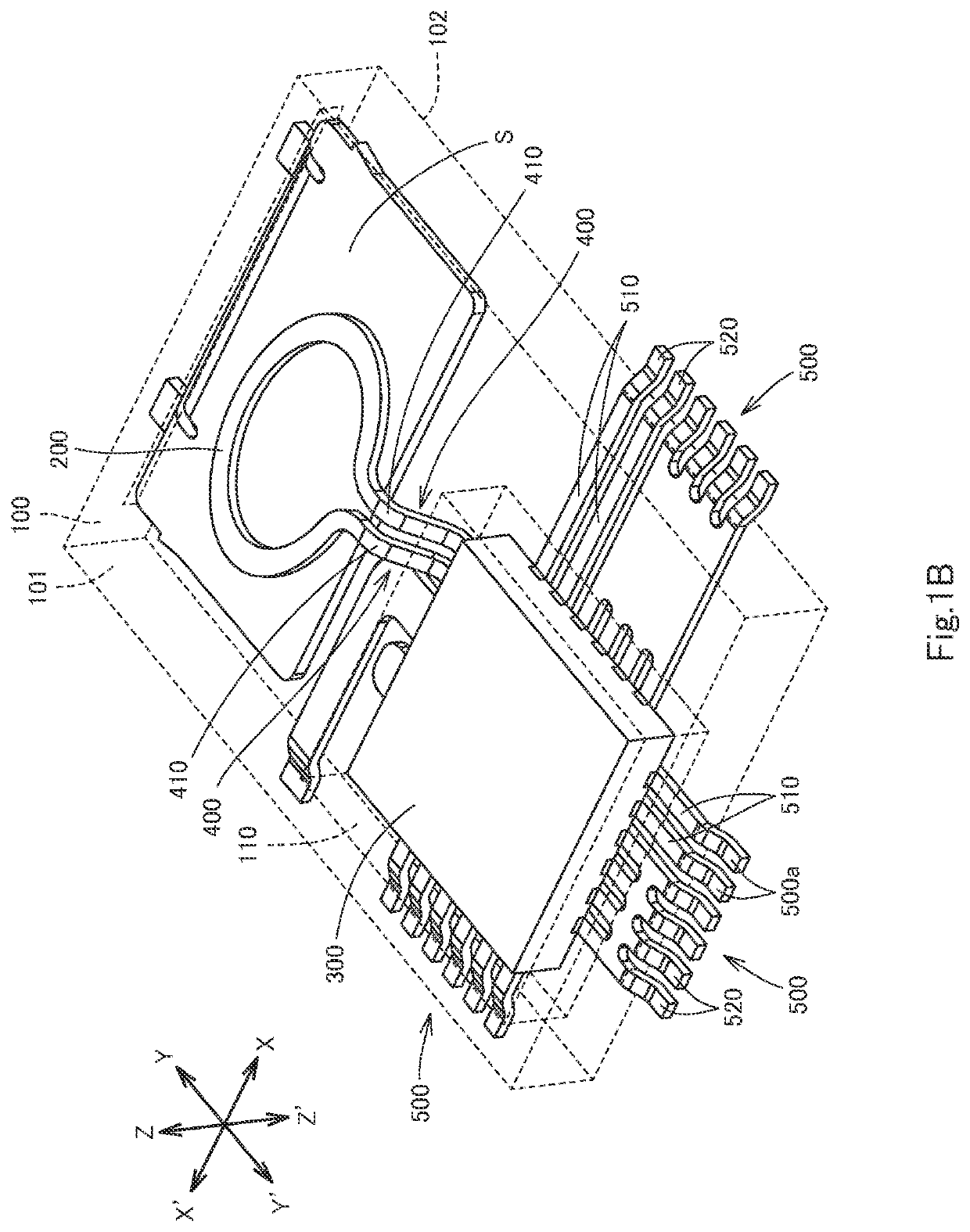
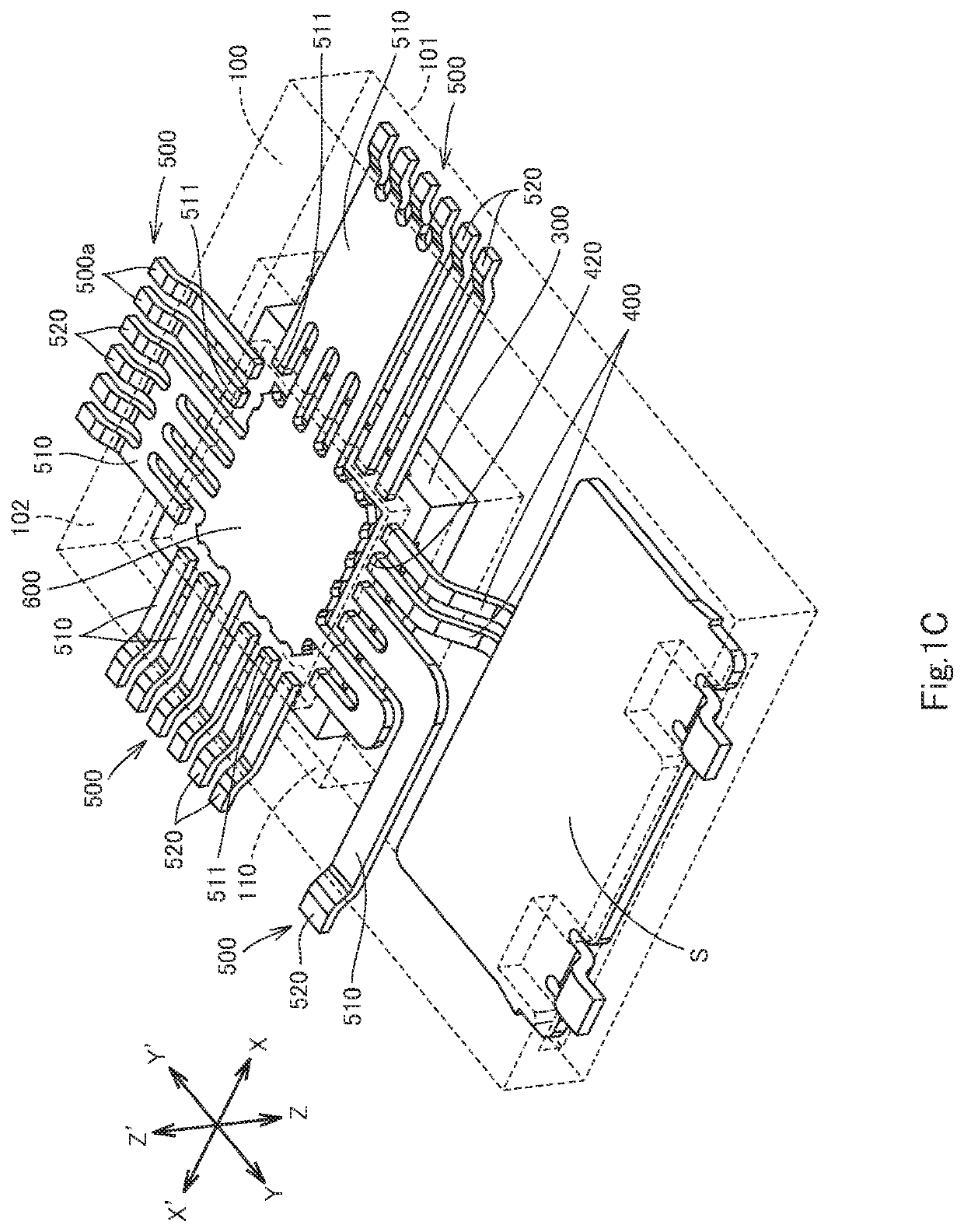
[0055]The following describes a contactless communication module M1 (also referred to hereinafter as module M1) according to a first embodiment of the invention, with reference to FIGS. 1A to 2B. The module M1 is adapted to contactlessly communicate with a partner communication device (not shown). The Z-Z′ direction indicated in FIGS. 1A to 1D is the thickness direction of the module M1 and corresponds to the first direction in the claims. The Z direction corresponds to one side of the first direction and the Z′ direction corresponds to the other side of the first direction. The Y-Y′ direction indicated in FIGS. 1A to 1D is the longitudinal direction of the module M1 and corresponds to the second direction in the claims. The Y-Y′ direction is orthogonal to the Z-Z′ direction. The X-X′ direction indicated in FIGS. 1A to 1C is the transverse direction of the module M1. The X-X′ direction is orthogonal to the Z-Z′ and Y-Y′ directions.

[0056]The module M1 includes a base 100 (package), a...

second embodiment

[0097]The following describes a contactless communication module M1′ (also referred to hereinafter as a module M1′) according to a second embodiment of the invention with reference to FIG. 3A. FIG. 3A also indicates the Z-Z′ and Y-Y′ directions in a similar manner to FIG. 1D.

[0098]The module M1′ is different from the module M1 in that the module M1′ does not include the island 600 but further includes a circuit board 700 (third circuit board). Otherwise the module M1′ has substantially the same configuration as that of the module M1. The module M1′ will now be described focusing on the differences from the module M1 and omitting overlapping descriptions.

[0099]The circuit board 700 is a rigid circuit board, a flexible circuit board, or a rigid flexible circuit board. The at least one semiconductor component 300 is mounted on the mounting face of the circuit board 700. The mounting face of the circuit board 700 may be either a Z-direction-side face or a Z′-direction-side face of the c...

third embodiment

[0110]The following describes a contactless communication module M1″ (also referred to hereinafter as a module M1″) according to a third embodiment of the invention with reference to FIG. 3B. FIG. 3B indicates the Z-Z′ and Y-Y′ directions in a similar manner to FIG. 1D.

[0111]The module M1″ differs from the module M1′ in that the module M1″ includes a circuit board 700′ (third circuit board) in place of the external connection 500 and the circuit board 700. Otherwise the module M1″ has substantially the same configuration as that of the module M1′. The module M1″ will now be described focusing on the differences from the module M1′ and omitting overlapping descriptions.

[0112]The circuit board 700′ has substantially the same configuration as that of the circuit board 700, except that the end portion on the Y′-direction side of the circuit board 700′ protrudes out of the base 100. The circuit board 700′ includes an external connection 710′. The external connection 710′ includes a first...


PUM


Abstract

A contactless communication module with improved communication accuracy is provided. A module M1 includes a base 100, an antenna 200, a semiconductor component 300, an internal connection 400, and an external connection 500. A partner communication device can be disposed at a short distance from, and on the Z-direction side relative to, the base 100. The antenna 200 is provided at the base 100, at a first height position such as to be able to contactlessly communicate with the partner communication device. The semiconductor component 300 is provided at the base 100, at the first height position or a second height position. The second height position is located on the Z′-direction side relative to the first height position. The internal connection 400 electrically connects the antenna 200 and the semiconductor component 300. The first portion 510 of the external connection 500 is provided at the base 100 and electrically connected to the semiconductor component 300. The second portion 520 of the external connection 500 protrudes out of the base 100.

Description

CROSS-REFERENCE TO RELATED APPLICATIONS[0001]The present application is a continuation application of U.S. patent application Ser. No. 16 / 061,594, filed Jun. 12, 2018, which is a National Stage filing of International Application No. PCT / JP2016 / 083078, filed Nov. 8, 2016, which in-turn claims priority from Japanese Patent Application No. 2015-248654, filed Dec. 21, 2015, and from Japanese Patent Application No. 2016-093091, filed May 6, 2016, all of which are incorporated herein, by reference, in their entireties.BACKGROUND OF THE INVENTIONTechnical Field[0002]The invention relates to a contactless communication module that performs communication in a contactless manner.Background Art[0003]In contactless communication, the communication accuracy greatly depends on design of a communication electric circuit, such as a semiconductor chip and an antenna. In particular, it is more difficult to design the communication electric circuit as the communication speed of contactless communicat...

Claims


Application Information

Patent Timeline
Patent Type & Authority Applications(United States)
IPC IPC(8): H01L23/66H04B5/02H04B5/00H01L23/495H01L23/50H01L23/12
CPCH01L23/66H04B5/02H04B5/0081H04B5/0031H01L23/49861H01L23/50H01L23/12H01L2223/6677H04B5/0037H01L23/49541H01L23/13H05K1/0243H05K1/14H05K2203/1327H01L25/0652H01L23/4985H01L23/49551H01L2223/6644
Inventor KONDO, HAYATO
Owner HOSIDEN CORP
Why Eureka
Try Eureka