Smartcard comprising a fingerprint sensor and method for manufacturing the smartcard

Active Publication Date: 2021-07-22
FINGERPRINT CARDS ANACATUM IP AB
View PDF0 Cites 1 Cited by
  • Summary
  • Abstract
  • Description
  • Claims
  • Application Information

AI Technical Summary

Benefits of technology

[0012]The present invention is based on the realization that by means of the claimed method, a cavity providing a number of advantages may be formed in a smartcard in a simple and efficient manner. In particular, by forming the cavity first and subsequently depositing the hydrophobic material, the extension of the hydrophobic material is limited by the cavity, meaning that there is no specific requirement for a mask to define where the hydrophobic material is provided. It is sufficient to control the amount of material deposited, and to control to deposition location with sufficient accuracy so that the material ends up in the cavity. Accordingly, the claimed manufacturing method can be performed with fewer method steps and with lower requirements on precision compared to if a coating was to be applied on a planar surface.
[0013]Furthermore, the described cavity provides a number of advantages for the smartcard as a whole. One advantage is that the cavity leads to improved sensitivity of the fingerprint sensor since the distance between a finger placed in the cavity of the sensing elements is reduced compared to if no cavity would be present. The cavity may also be referred to as a recess, indentation or the like. It is furthermore assumed that the fingerprint sensor is placed as close as possible to the outer surface of the smartcard.
[0014]Moreover, the cavity

Problems solved by technology

However, capacitive fingerprint sensing devices are typically sensitive to contaminants located between the capacitive sensing elements of the sensor and the finger to be measured.
For example, residual fingerprints on the sensing surface may reduce the accuracy of the sensing device,

Method used


Image

  • Smartcard comprising a fingerprint sensor and method for manufacturing the smartcard
  • Smartcard comprising a fingerprint sensor and method for manufacturing the smartcard
  • Smartcard comprising a fingerprint sensor and method for manufacturing the smartcard

Examples


Example

[0033]In the present detailed description, various embodiments of the system and method according to the present invention are mainly described with reference to a smartcard comprising a capacitive fingerprint sensor embedded therein. However, the described method may also be employed for other types of biometric devices suitable for use in a smartcard.

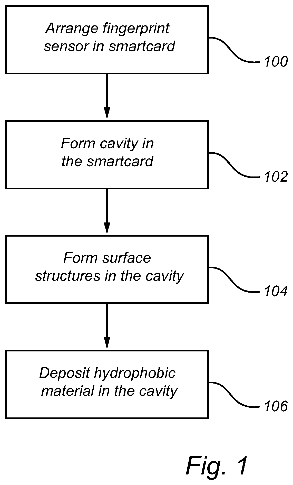
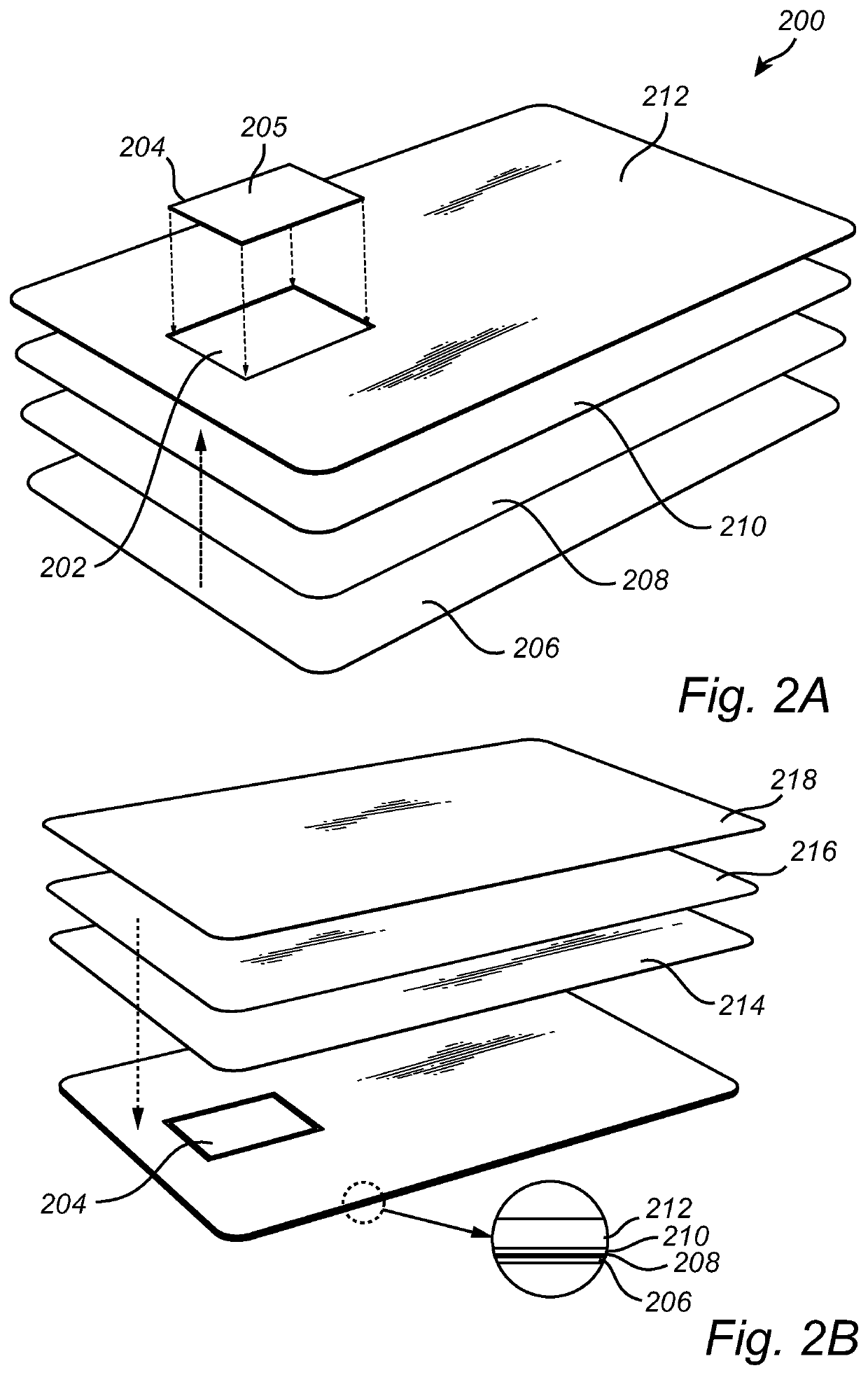
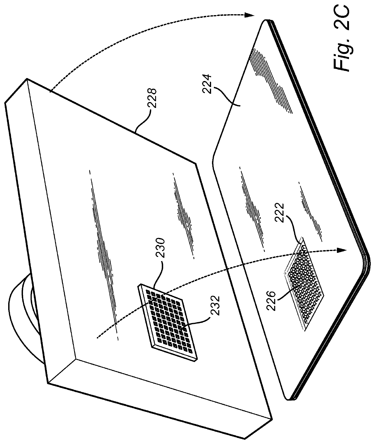
[0034]FIG. 1 is a flow chart outlining the general steps of a method according to an embodiment of the invention. The method will be described with further reference to FIGS. 2A-D schematically illustrating general method steps of a method of manufacturing a smart card according to an embodiment of the invention.

[0035]First, a smartcard body 200 comprising an opening 202 for receiving a fingerprint sensor module 204 is provided. A smartcard is typically a laminated structure comprising a plurality of layers where many variations are possible. In the present description, only the layers most relevant for the described method will be il...


PUM


Abstract

Method for manufacturing a smartcard comprising a fingerprint sensor, the method comprising: arranging a fingerprint sensor module in an opening of a carrier layer of a smartcard body; forming a cavity in the smartcard in an area corresponding to a sensing area of the fingerprint sensor module; forming a plurality of surface structures in the cavity of the smartcard; depositing a liquid hydrophobic material in the cavity to at least partially cover the surface structures and a smartcard manufactured according to the described method.

Description

FIELD OF THE INVENTION[0001]The present invention relates to a smartcard comprising a biometric sensor and to a method for manufacturing a smartcard comprising a biometric sensor.BACKGROUND OF THE INVENTION[0002]As the development of biometric devices for identity verification, and in particular of fingerprint sensing devices, has led to devices which are made smaller, cheaper and more energy efficient, the possible applications for such devices are increasing.[0003]In particular fingerprint sensing has been adopted more and more in, for example, consumer electronic devices, due to small form factor, relatively beneficial cost / performance factor and high user acceptance.[0004]Capacitive fingerprint sensing devices, built based on CMOS technology for providing the fingerprint sensing elements and auxiliary logic circuitry, are increasingly popular as such sensing devices can be made both small and energy efficient while being able to identify a fingerprint with high accuracy. Thereby...

Claims


Application Information

Patent Timeline
IPC IPC(8): G06K19/07G06K19/077
CPCG06K19/0718G06K19/07722G06K19/077
Inventor LUNDAHL, KARLLIGNIER, OLIVIER
Owner FINGERPRINT CARDS ANACATUM IP AB
Why Eureka
Try Eureka