Semiconductor device and manufacturing method therefor

a manufacturing method and semiconductor technology, applied in semiconductor devices, electrical devices, nanotechnology, etc., can solve the problems of difficult recrystallization for restoring crystal defects, unlikely to become significant problems, and occurrence of leak currents that are unlikely to become a problem, so as to reduce the occurrence of leak currents and reduce the excessive increase of resistance of channel units

Active Publication Date: 2021-07-29
SONY SEMICON SOLUTIONS CORP
View PDF4 Cites 1 Cited by
  • Summary
  • Abstract
  • Description
  • Claims
  • Application Information

AI Technical Summary

Benefits of technology

[0007]An object of the present disclosure, therefore, is to provide a semiconductor device and a manufacturing method therefor, the semiconductor device being configured and structured to be capable of reducing the occurrence of the leak current and reducing the excessive increase of the resistance of the channel unit.

Problems solved by technology

In this case, performing the impurity profile control based on the ion implantation causes crystal defects in source / drain regions and any other portion.
Unfortunately, recrystallization for restoring the occurred crystal defects is difficult in, for example, a semiconductor device having a Fin structure, as described later.
A power supply voltage Vdd for semiconductor devices tends to be lowered, and in the case of such a lowered power supply voltage Vdd, the occurrence of such a leak current is unlikely to become a significant problem.
However, the occurrence of such a leak current is still a significant problem in the case of a high power supply voltage Vdd, for example, a voltage from 1.5 to 3.3 volts.

Method used


Image

  • Semiconductor device and manufacturing method therefor
  • Semiconductor device and manufacturing method therefor
  • Semiconductor device and manufacturing method therefor

Examples


embodiment 1

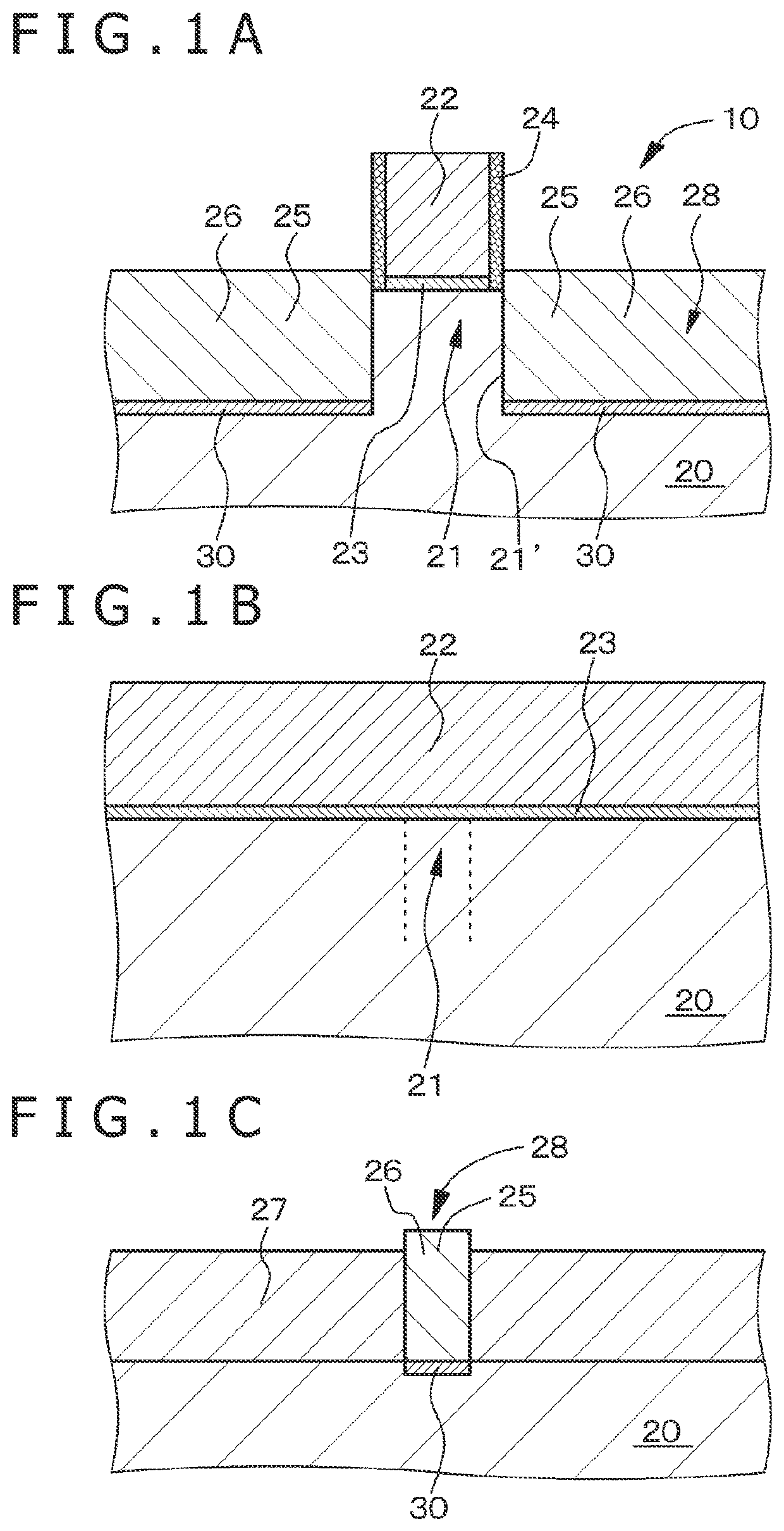
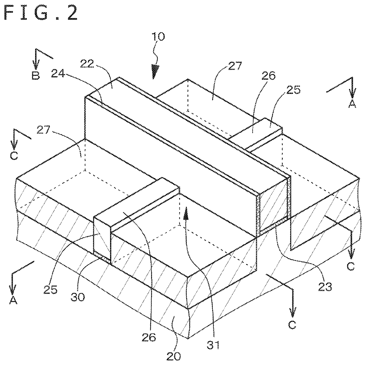
[0059]This embodiment 1 relates to a semiconductor device and a manufacturing method therefor according to the present disclosure. FIGS. 1A, 1B, and 1C illustrate schematic partial cross-sectional views of a semiconductor device according to the embodiment 1, taken along arrows A-A, B-B, and C-C of FIG. 2, and FIG. 2 illustrates a schematic partial perspective view of the semiconductor device according to the embodiment 1.

[0060]A semiconductor device 10 according to the embodiment 1 and embodiments 2 and 3 described later includes a channel portion 21, a gate electrode 22 disposed opposite the channel portion 21 via a gate insulating film 23, and source / drain regions 25 disposed at both edges of the channel portion 21. The source / drain regions 25 include semiconductor layers 26 that have a first conductivity type (specifically, for example, n+) and that are formed inside recessed portions 28 disposed on a base body 20. Impurity layers (high-concentration impurity layers) 30 having a...

embodiment 2

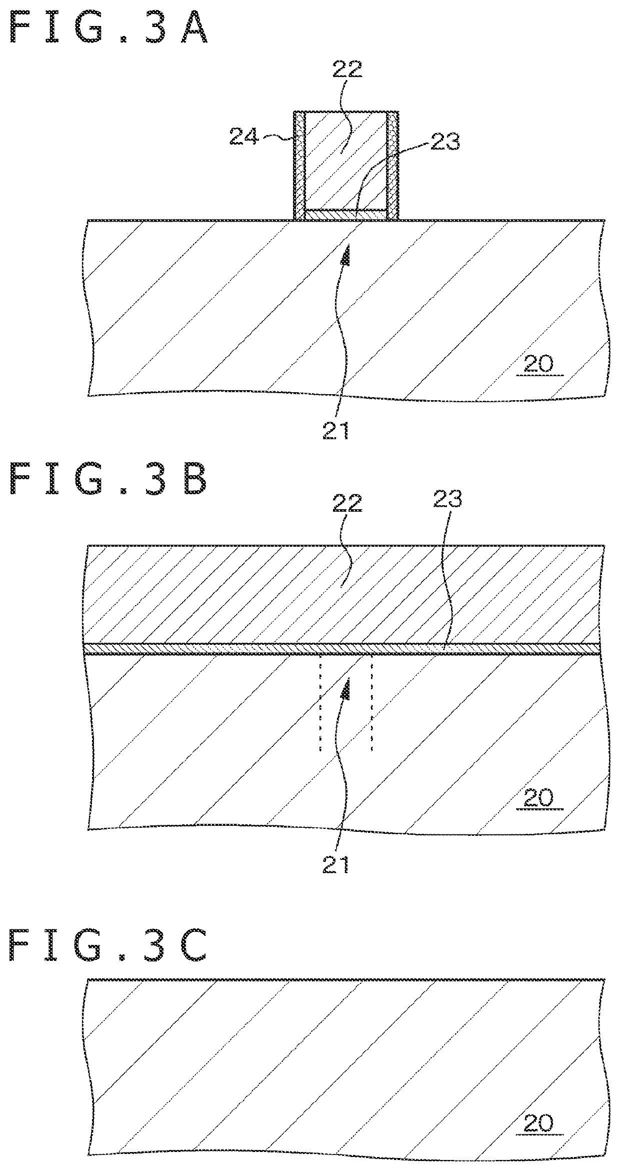
[0076]This embodiment 2 is a modification of the embodiment 1. In the semiconductor device according to the embodiment 1, the high-concentration impurity layers are unlikely to be formed on boundary regions 21′ between the channel portion 21 and the source / drain regions 25. However, there may occur a situation in which the high-concentration impurity layers (the second impurity layers 31) are, albeit only slightly, formed on the boundary regions 21′ between the channel portion 21 and the source / drain regions 25 although the occurrence depends on conditions for forming the impurity layers 30 and any other condition (see FIG. 22A, which is a schematic partial cross-sectional view of another example of the semiconductor device according to the embodiment 1, taken in a way similar to that along the arrow A-A of FIG. 2). In the embodiment 2, the cross-sectional shape of each of side faces 21A of the channel portion 21 that are opposite to side faces of the semiconductor layers 26 is form...

embodiment 3

[0080]This embodiment 3 is also a modification of the embodiment 1. In the semiconductor device according to the embodiment 2, since the cross-sectional shape of each of the side faces 21A of the channel portion 21 that are opposite to the side faces of the semiconductor layers 26 has the recessed shape, the high-concentration impurity layers are more unlikely to be formed on the boundary regions 21′ between the channel portion 21 and the source / drain regions 25. However, there may occur a situation in which the high-concentration impurity layers (the second impurity layers 31) are, albeit only slightly, formed on a lower portion of the boundary regions 21′ between the channel portion 21 and the source / drain regions 25 although the occurrence depends on conditions for forming impurity layers 30 and any other condition (see FIG. 22B, which is a schematic partial cross-sectional view of another example of the semiconductor device according to the embodiment 2, taken in a way similar t...


PUM

PropertyMeasurementUnit
voltageaaaaaaaaaa
conductivityaaaaaaaaaa
thicknessaaaaaaaaaa

Abstract

A semiconductor device according to the present disclosure includes a channel portion, a gate electrode disposed opposite the channel portion via a gate insulating film, and source/drain regions disposed at both edges of the channel portion. The source/drain regions include semiconductor layers that have a first conductivity type and that are formed inside recessed portions disposed on a base body. Impurity layers having a second conductivity type different from the first conductivity type are formed between the base body and bottom portions of the semiconductor layers.

Description

TECHNICAL FIELD[0001]The present invention relates to a semiconductor device and a manufacturing method therefor.BACKGROUND ART[0002]Conventional planar type semiconductor devices (specifically, MOSFETs), schematic partial cross-sectional view thereof being illustrated in FIG. 23, have a significant problem of the occurrence of a reverse bias p-n junction leak current (hereinafter simply referred to as a “leak current”). Note here that FIG. 23 illustrates this leak current using white arrows. Further, in order to reduce the occurrence of such a leak current, impurity profile control based on ion implantation is effective (see, for example, Japanese Patent Laid-open No. 2009-026940). In this case, performing the impurity profile control based on the ion implantation causes crystal defects in source / drain regions and any other portion. Unfortunately, recrystallization for restoring the occurred crystal defects is difficult in, for example, a semiconductor device having a Fin structure...

Claims


Application Information

Patent Timeline
Patent Type & Authority Applications(United States)
IPC IPC(8): H01L29/06H01L29/78H01L21/3115
CPCH01L29/0673H01L21/31155H01L29/7851H01L29/785H01L29/0847H01L29/0646H01L29/775H01L29/66795H01L29/78696H01L29/42392B82Y10/00H01L29/1079H01L29/66439
Inventor TOMIDA, KAZUYUKI
Owner SONY SEMICON SOLUTIONS CORP
Why Eureka
Try Eureka