Micro light emitting diode display panel

a light-emitting diode and display panel technology, applied in the field of micro light-emitting diode display panel, can solve the problems of deteriorating the image quality of the display panel, unable to be lit up, and the number of sub-pixel regions is less, so as to improve the probability of success bonding, excellent production yield and image quality

Pending Publication Date: 2021-09-09
PLAYNITRIDE
View PDF0 Cites 3 Cited by
  • Summary
  • Abstract
  • Description
  • Claims
  • Application Information

AI Technical Summary

Benefits of technology

[0006]The invention provides a micro light emitting diode chip, which can make the probability of the success bonding of the display panel applying the abovementioned micro light emitting diode chip high, and having excellent production yield and image quality.

Problems solved by technology

However, when the electrodes of the micro LED are bonded to the pads on the backplane of the display panel, it is not easy to align the electrodes of the micro LED to the pads on the backplane and lower the production yield of the display panel or deteriorate the image quality of the display panel.
If it is found that one of the micro LEDs in the sub-pixel region is defective product when the display panel is tested, for example, a micro LED in the sub-pixel region can't be lit up.
However, such the solution method may make the sub-pixel region being overly large, the number of the sub-pixel regions is less, and the overall resolution of the display panel is then limited.

Method used


Image

  • Micro light emitting diode display panel
  • Micro light emitting diode display panel
  • Micro light emitting diode display panel

Examples


Embodiment Construction

[0048]Reference will now be made in detail to the present preferred embodiments of the invention, examples of which are illustrated in the accompanying drawings. Wherever possible, the same reference numbers are used in the drawings and the description to refer to the same or like parts.

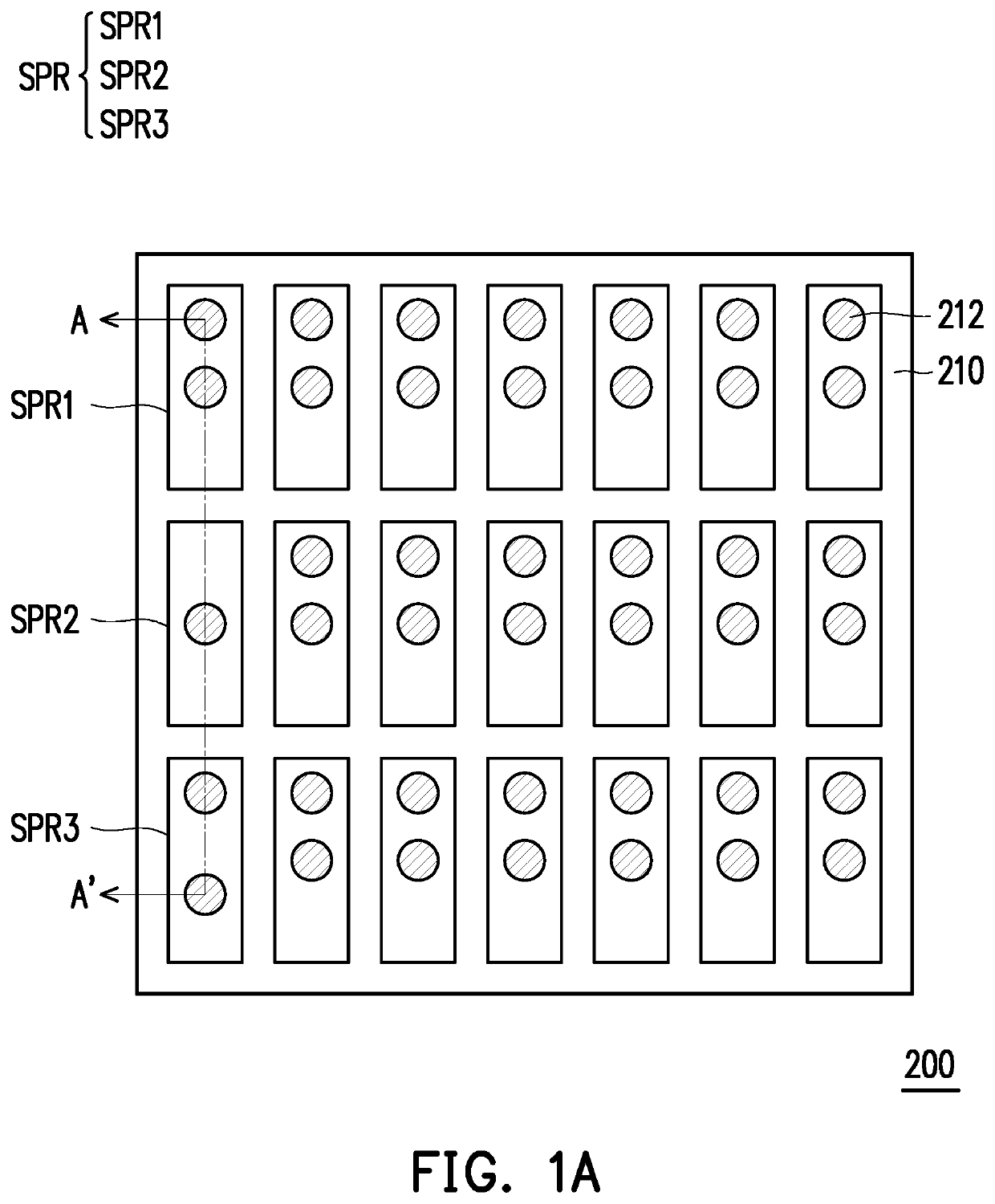
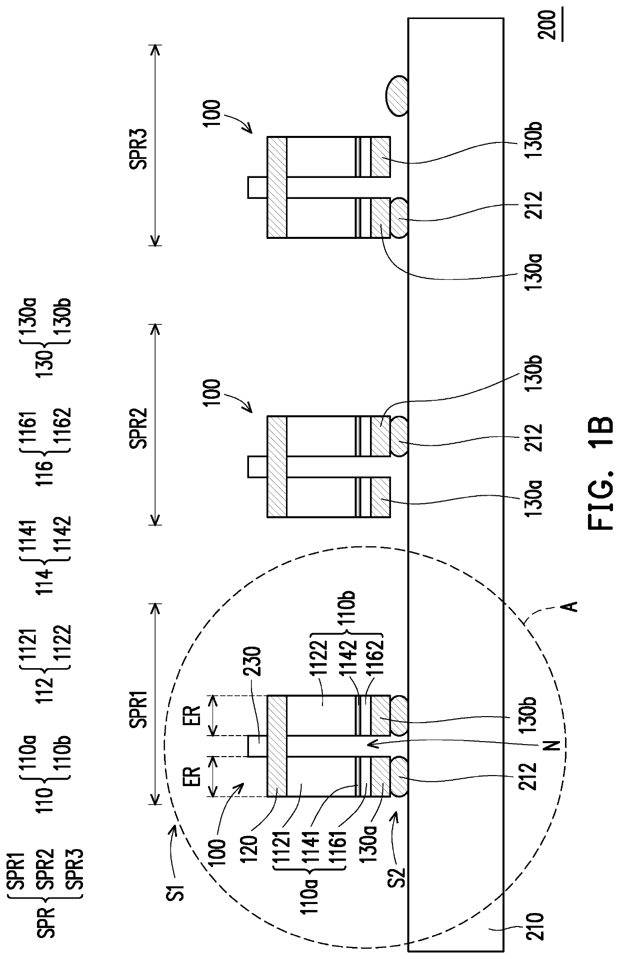
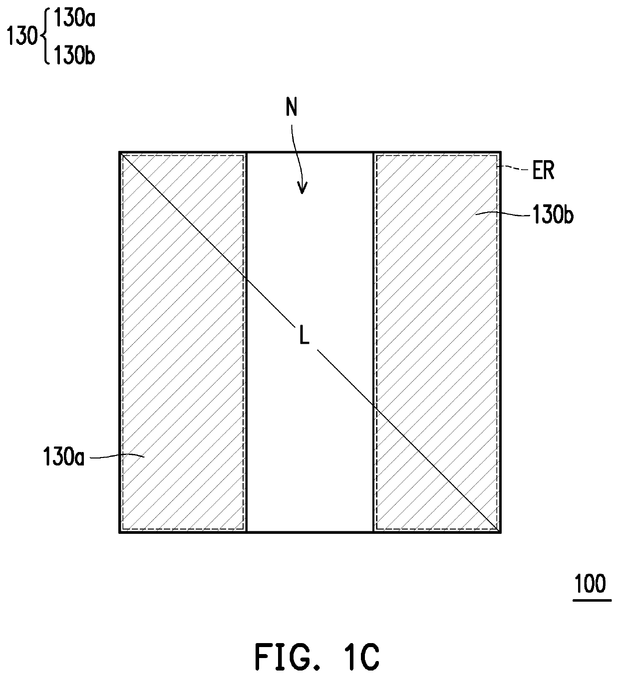
[0049]FIG. 1A is a schematic top view of the display panel according to an embodiment of the invention. FIG. 1B is a schematic cross-sectional view taken along a section line A-A′ in FIG. 1A. FIG. 1C is a bottom view of the micro light emitting diode chip of the display panel in FIG. 1A. It should be noted that, for the clear illustration, the micro light emitting diode chip and other layer structures are omitted in FIG. 1A, only the bonding location of the sub-pixel region and the micro light emitting diode chip are illustrated in the FIG. 1A. FIG. 1D is an enlargement view illustrating the region A in FIG. 1A.

[0050]Referring to FIG. 1A and FIG. 1B, in the embodiment, the display panel 200 includes ...


PUM

PropertyMeasurementUnit
lengthaaaaaaaaaa
areaaaaaaaaaaa
electricalaaaaaaaaaa

Abstract

A micro light emitting diode display panel includes a backplane and a plurality of micro light emitting diode chips. The backplane includes a plurality first electrode lines and a plurality of second electrode lines. The first electrode lines and the second electrode lines define a plurality of sub-pixel regions arranged in an array form. The micro light emitting diode chips are disposed on the backplane and respectively located in the sub-pixel regions. Each of the micro light emitting diode chips has a first electrode, a plurality of second electrodes and a plurality of light-emitting regions. The first electrode is boned to one of the first electrode lines, and the second electrodes are boned to one of the second met lines. In a defect sub-pixel region, the electrical connection between one of the second electrodes and the corresponding one of the second electrode lines is cut to isolate.

Description

CROSS-REFERENCE TO RELATED APPLICATION[0001]This application is a continuation-in-part application of and claims the priority benefit of U.S. application Ser. No. 16 / 935,163, filed on Jul. 21, 2020, now allowed, which is a continuation application of and claims the priority benefit of U.S. application Ser. No. 15 / 866,473, filed on Jan. 10, 2018, now patented. The prior U.S. application Ser. No. 15 / 866,473 claims the priority benefit of Taiwan application serial no. 106100760, filed on Jan. 10, 2017. The entirety of each of the above-mentioned patent applications is hereby incorporated by reference herein and made a part of this specification.BACKGROUND OF THE INVENTION1. Field of the Invention[0002]The present invention relates to a light emitting diode chip and display panel, and particularly relates to a micro light emitting diode (μLED) chip and a display panel having the micro light emitting diode chip.2. Description of Related Art[0003]The micro LED (μLED) has self-luminous dis...

Claims


Application Information

Patent Timeline
Patent Type & Authority Applications(United States)
IPC IPC(8): H01L33/06H01L27/146C30B25/18G09G3/32H01L25/075H01L27/12C30B29/40H01L27/15
CPCH01L33/06H01L27/14692C30B25/183G09G3/32H01L25/0753H01L33/08C30B29/406H01L27/1259H01L27/153G09G2300/0452H01L27/1225H01L25/167H01L33/382H01L33/62
Inventor LO, YU-YUNWU, BO-WEIYANG, SHIANG-NINGTSAI, CHANG-FENG
Owner PLAYNITRIDE
Why Eureka
Try Eureka