

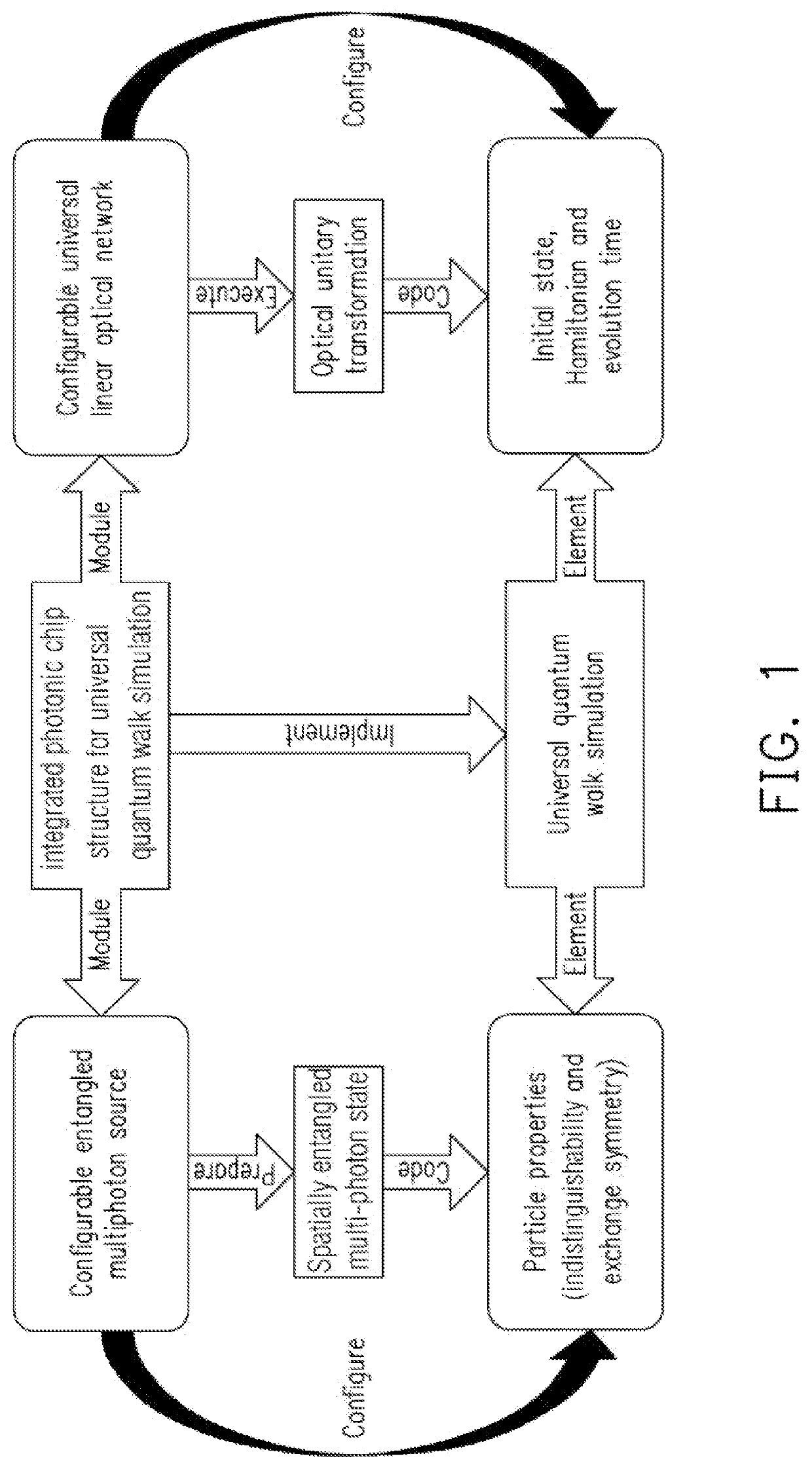
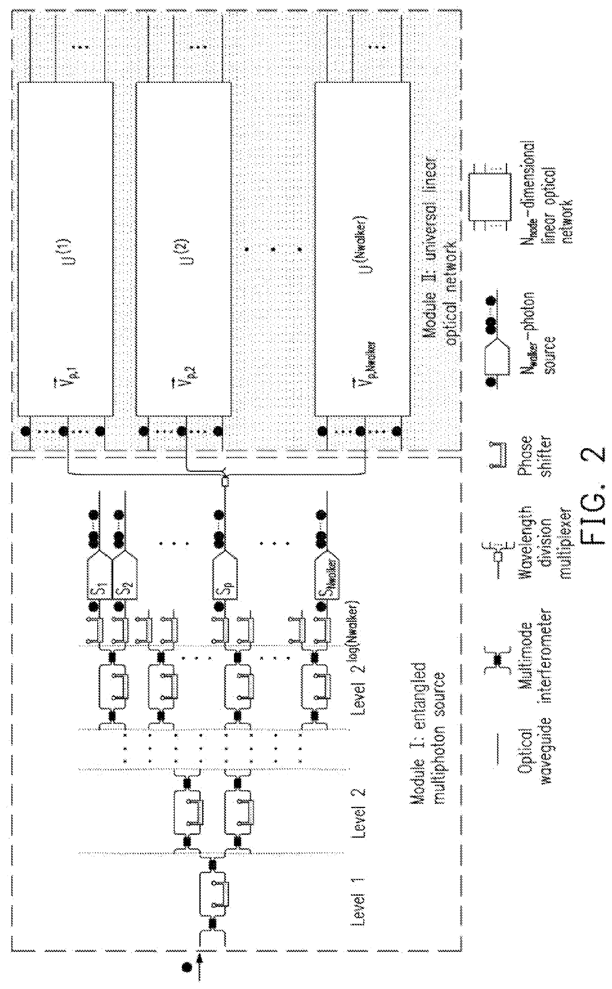
Integrated photonic chip structure for universal quantum walk simulation
- Summary
- Abstract
- Description
- Claims
- Application Information
AI Technical Summary
Benefits of technology
Problems solved by technology
Method used
Image

Examples
example 1
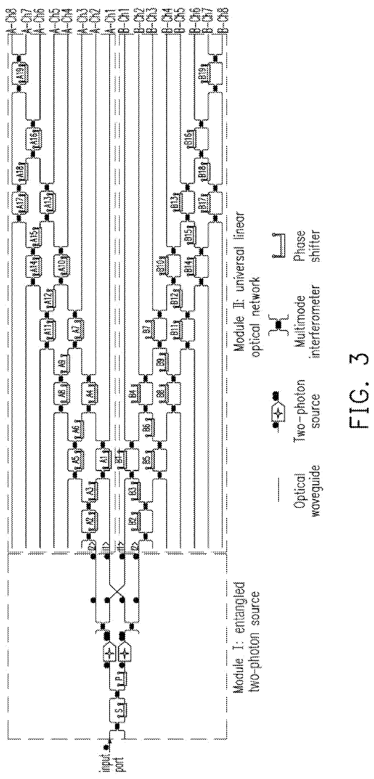
[0029]A photonic chip structure for universal quantum walk simulation with two quantum particles starting from nodes 1 and 2 on a 8-node graph G, as shown in FIG. 3, consists of two modules, with the first half being a reconfigurable entangled two-photon source module I, and the second half being a universal linear optical network module II composed of two 8-dimensional universal linear optical networks A and B, with each optical network capable of implementing universal linear optical unitary transformation with fixed input ports (1 and 2 here). The whole chip has 40 controllable phase shifters. When the chip is used to simulate distribution results of two particles quantum walks with the parameters of indistinguishability γ, exchange symmetry ϕ, walk time t and walk Hamiltonian HG and starting from nodes 1 and 2, the chip needs to be configured and manipulated as follows:
[0030]1. Two phase shifters S and P in the reconfigurable entangled multiphoton source module I are configured ...
PUM
 Abstract
Description
Claims
Application Information