
Method and apparatus for avoiding parasitic oscillation in a parallel semiconductor switch

Inactive Publication Date: 2021-12-02
MURATA MFG CO LTD
View PDF0 Cites 0 Cited by
  • Summary
  • Abstract
  • Description
  • Claims
  • Application Information

AI Technical Summary

Benefits of technology

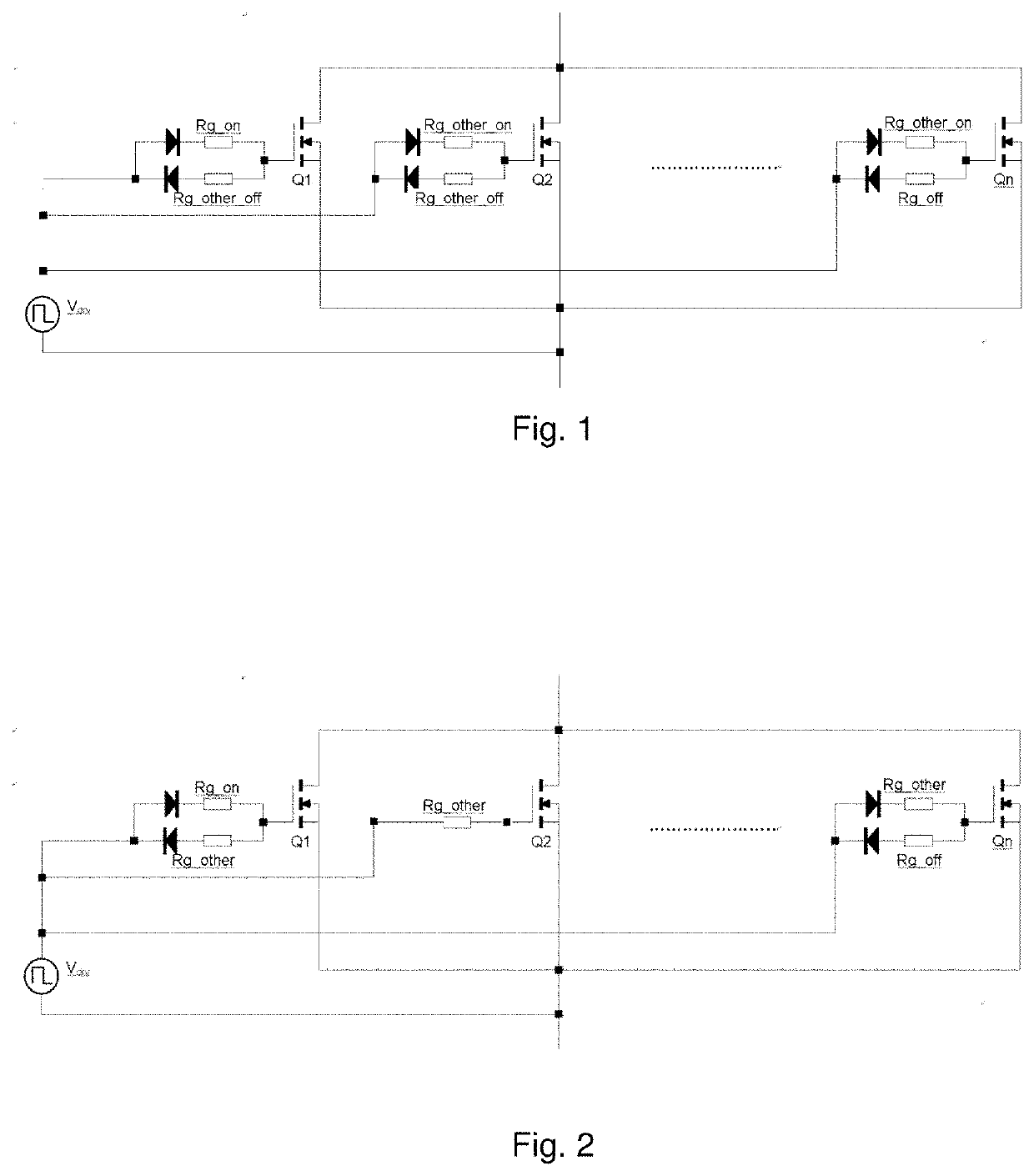
The present invention provides a way to prevent parasitic oscillation between power components when they are operated in parallel. This is achieved by introducing unbalanced driving impedances into parallel semiconductor switches. The invention ensures that only one of the plurality of power components coupled in parallel is turned on, and only one of the plural power components coupled in parallel is turned off during a switch transition period. This eliminates the need for impedance matching, minimizing the impact on switch characteristics such as switch loss and switch speed.

Problems solved by technology

It is not uncommon that power supplies operated by parallel switches fail to operate.
The problems seem to occur randomly.
The parasitic oscillation may generate internal overstress, which is not easy to observe outside the component.
When parasitic oscillation occurs, the internal overstress may destroy a relatively weak control terminal (such as a junction between a gate of the MOSFET and a source of the MOSFET), leading to problems.
In a switch transition period, switching current is redistributed among power components, triggering parasitic oscillation.
Therefore, parasitic oscillation is prone to occur in parallel operations of power components.
The parasitic oscillation depends on parasitic parameters of the power components operated in parallel, such that potential problems may not be observed in a development stage.
However, problems usually occur after the power components are in production.
This leads to potential reliability problems in the parallel operation of power components.
However, the solution is impractical in mass production.
According to another existing solution, the driving resistance is increased to suppress the parasitic oscillation, but this will increase switching loss and switching duration.

Method used


Image

  • Method and apparatus for avoiding parasitic oscillation in a parallel semiconductor switch

Examples


Embodiment Construction

[0034]Preferred embodiments of the present invention will be described in detail below with reference to the drawings. The same or corresponding elements and component are denoted by the same reference characters in the drawings.

[0035]The present invention should not be limited to the specific preferred embodiments described below. In addition, for brevity, detailed descriptions of well-known technologies that are not directly related to preferred embodiments of the present invention are omitted to prevent confusion in the understanding of the preferred embodiments of the present invention.

[0036]In order to avoid parasitic oscillation in a parallel semiconductor switch, preferred embodiments of the present invention propose to ensure that only one of a plurality of power components operated in parallel is turned on, and only one of the plurality of power components operated in parallel is turned off in a switch transition period of a parallel semiconductor switch. That is, only one ...


PUM


Abstract

A method for avoiding parasitic oscillation in a parallel semiconductor switch includes allowing only one of the plurality of power components to control a turn-on transition of the semiconductor switch and allowing only one of the plurality of power components to control a turn-off transition of the semiconductor switch, by setting unbalanced driving impedances for the plurality of power components coupled in parallel. Parasitic oscillation in a switch transition may be avoided without impedance matching, and the switch transition may provide a relatively small impact on switch characteristics.

Description

CROSS REFERENCE TO RELATED APPLICATIONS[0001]This application claims the benefit of priority to Chinese Patent Application No. 202010486888.X filed Jun. 1, 2020. The entire contents of this application are hereby incorporated herein by reference.BACKGROUND OF THE INVENTION1. Field of the Invention[0002]The present disclosure relates to a parallel semiconductor switch, and more specifically, to a method and apparatus for avoiding parasitic oscillation in a parallel semiconductor switch.2. Description of the Related Art[0003]A switching mode power supply is a high-frequency apparatus for electric energy conversion, which periodically turns on and turns off an electronic switching component by using a power semiconductor component (including but not limited to metal semiconductor field effect transistors MOSFET, bipolar transistor BJT or insulated gate bipolar transistor IGBT, etc.) in a control circuit. Pulse modulation is implemented on an input voltage by the power semiconductor com...

Claims


Application Information

Patent Timeline
IPC IPC(8): H03K17/16H02M1/38
CPCH03K17/161H02M1/38H02M1/088H03K17/122H03K17/127H03K17/08122H03K17/08126H03K17/08128H03K17/163H03K17/168
Inventor LIU, CHUIPONG
Owner MURATA MFG CO LTD
Learn More