Method for avoiding parasitic oscillation in parallel semiconductor switches and corresponding device

A semiconductor and switching technology, applied in the field of parallel semiconductor switches, can solve the problems of increasing switching loss and switching time, unrealistic, etc., and achieve the effect of avoiding parasitic oscillation

Pending Publication Date: 2021-12-07
MURATA MFG CO LTD
View PDF0 Cites 0 Cited by
  • Summary
  • Abstract
  • Description
  • Claims
  • Application Information

AI Technical Summary

Problems solved by technology

[0006] An existing solution proposes to match all drive impedances of the power devices so that all power devices in parallel are turned on and off simultaneously, but this is impractical in mass production
[0007] Another existing solution proposes to increase the drive resistance to suppress parasitic oscillations, but this solution increases switching losses and switching time

Method used


Image

  • Method for avoiding parasitic oscillation in parallel semiconductor switches and corresponding device
  • Method for avoiding parasitic oscillation in parallel semiconductor switches and corresponding device
  • Method for avoiding parasitic oscillation in parallel semiconductor switches and corresponding device

Examples


Embodiment Construction

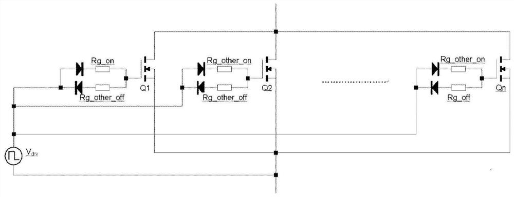
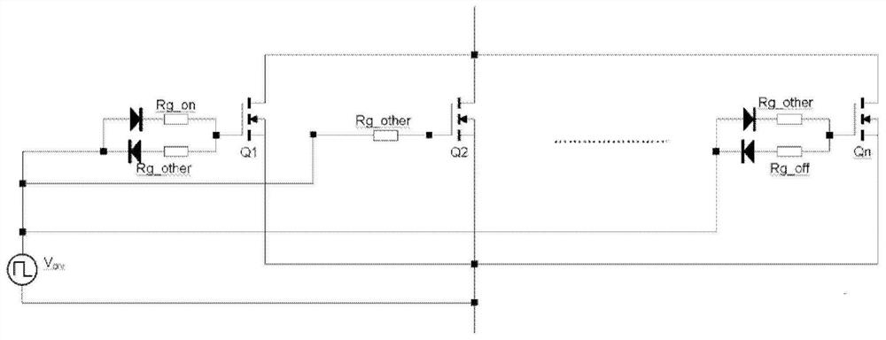
[0037] The solution of the present disclosure will be described in detail below in conjunction with the accompanying drawings and specific embodiments. It should be noted that the present disclosure should not be limited to the specific embodiments described below. In addition, for the sake of brevity, detailed descriptions of well-known technologies that are not directly related to the present disclosure are omitted to prevent confusion to the understanding of the present disclosure.

[0038] In order to avoid parasitic oscillations in parallel semiconductor switches, embodiments of the present disclosure propose to ensure that only one of multiple power devices operating in parallel is turned on and off during transitions of switching transitions of the parallel semiconductor switches. That is, only one power device controls the turn-on transition of the switch, and only one power device controls the turn-off transition of the switch.

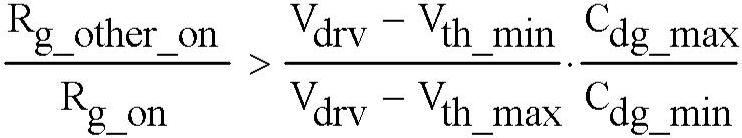
[0039] The power device for controlli...


PUM


Abstract

The embodiment of the invention provides a method for avoiding parasitic oscillation in parallel semiconductor switches and a corresponding device. According to the embodiment of the invention, the method comprises the step of setting unbalanced driving impedance for a plurality of power devices connected in parallel, so only one power device controls the opening transition of the switch and only one power device controls the closing transition of the switch. According to the embodiment of the invention, parasitic oscillation during the switching period of the switch is avoided, impedance matching is not needed, and the influence on the switching characteristic is small.

Description

technical field [0001] The present invention relates to parallel semiconductor switches, more particularly to methods and corresponding arrangements for avoiding parasitic oscillations in parallel semiconductor switches. Background technique [0002] Switching power supply is a high-frequency power conversion device, which mainly uses power semiconductor devices (including but not limited to metal semiconductor field effect transistor MOSFET, bipolar transistor BJT and insulated gate bipolar transistor IGBT, etc.), through the control circuit, Make the electronic switching device "turn on" and "turn off" periodically, let the power semiconductor device (hereinafter referred to as the power device) perform pulse modulation on the input voltage, so as to realize the function of voltage conversion, output voltage adjustment and automatic voltage regulation . Switching power supplies are therefore also called power converters. [0003] In applications that require high current...

Claims


Application Information

Patent Timeline
Patent Type & Authority Applications(China)
IPC IPC(8): H02M1/088
CPCH02M1/088H03K17/122H03K17/127H03K17/08122H03K17/08126H03K17/08128H03K17/163H03K17/168H02M1/38H03K17/161
Inventor 廖柱帮
Owner MURATA MFG CO LTD
Why Eureka
Try Eureka