Mixed compensation circuit, control method thereof, and display device

a compensation circuit and control method technology, applied in the field of display technologies, can solve problems such as poor stability and circuit failure to operate properly, and achieve the effects of improving compensation accuracy, simplifying compensation process, and improving circuit stability

Active Publication Date: 2021-12-30
SHENZHEN CHINA STAR OPTOELECTRONICS SEMICON DISPLAY TECH CO LTD
View PDF0 Cites 0 Cited by
  • Summary
  • Abstract
  • Description
  • Claims
  • Application Information

AI Technical Summary

Benefits of technology

[0037]By optimizing the pixel circuit architecture, there is no long-term NTFT with a positive relative voltage, which improves the stability of the circuit, while simplifying the compensation process and improving the accuracy of compensation.

Problems solved by technology

In other words, there is always a current flowing on the path of the four thin film transistors, so that the thin film transistor T4 operating under a large Vgs (relative voltage) voltage for a long time, however, the NTFT currently used for switching is usually made of an oxide semiconductor, which has poor stability, under long-term forward Vgs, reliability anomalies often occur, causing the circuit to fail to operate properly.

Method used


Image

  • Mixed compensation circuit, control method thereof, and display device
  • Mixed compensation circuit, control method thereof, and display device
  • Mixed compensation circuit, control method thereof, and display device

Examples


Embodiment Construction

[0045]In order to have a clearer understanding of the technical features, objects, and effects of the present disclosure, specific embodiments of the present disclosure will now be described in detail with reference to the figures.

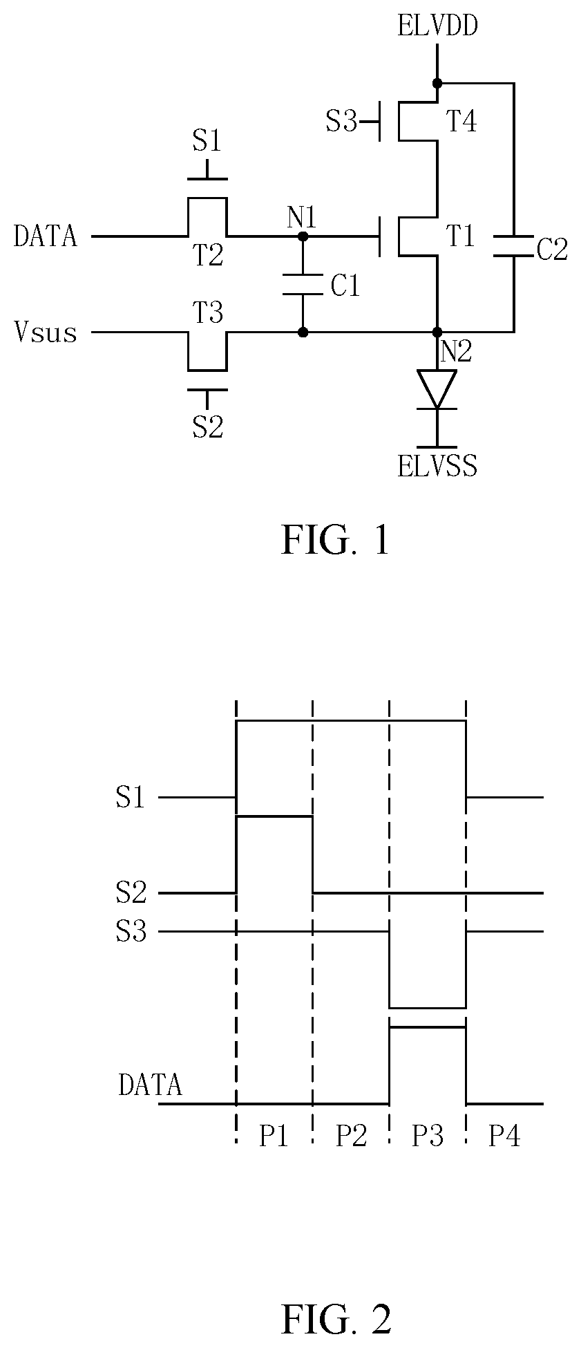
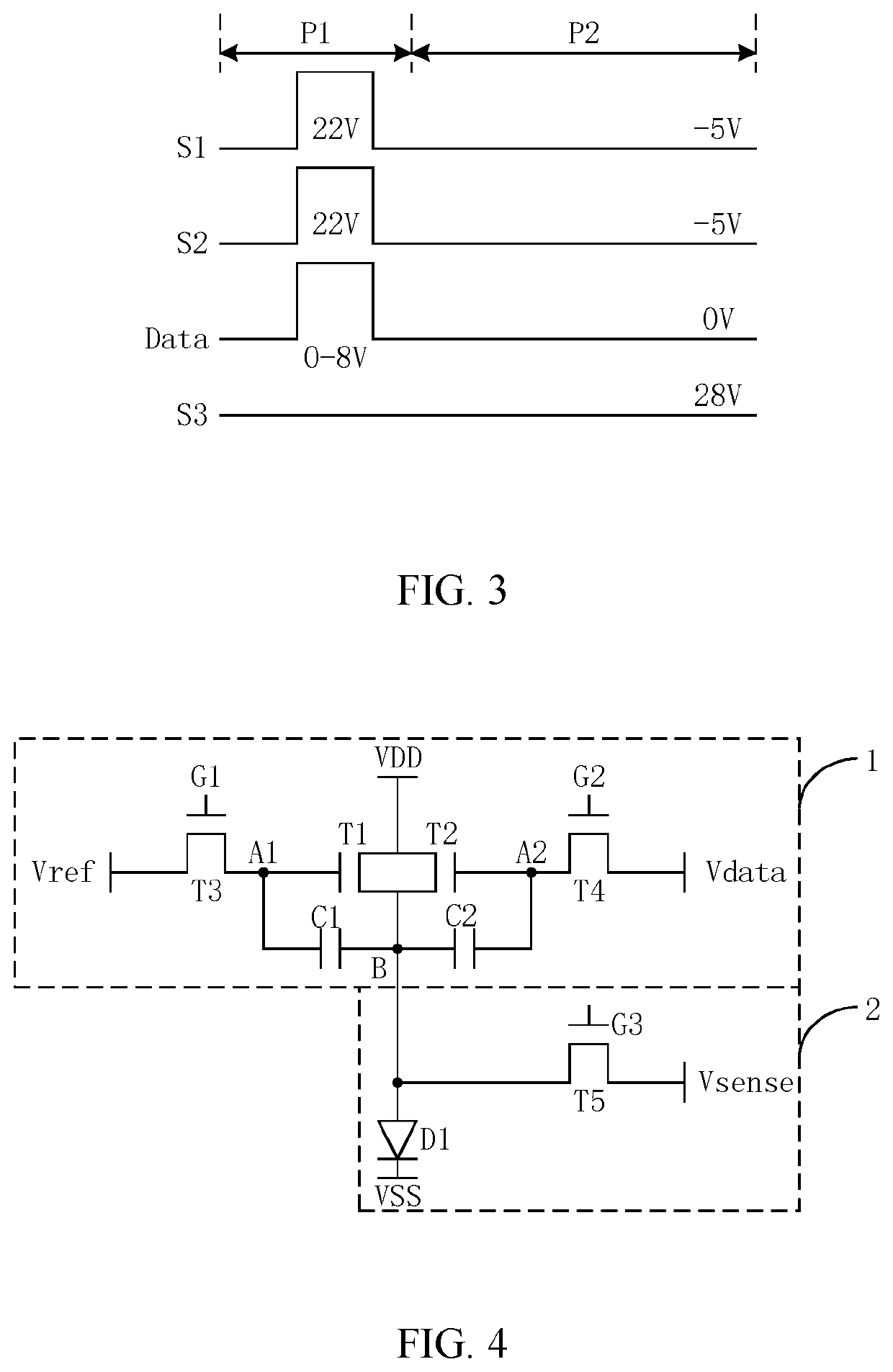
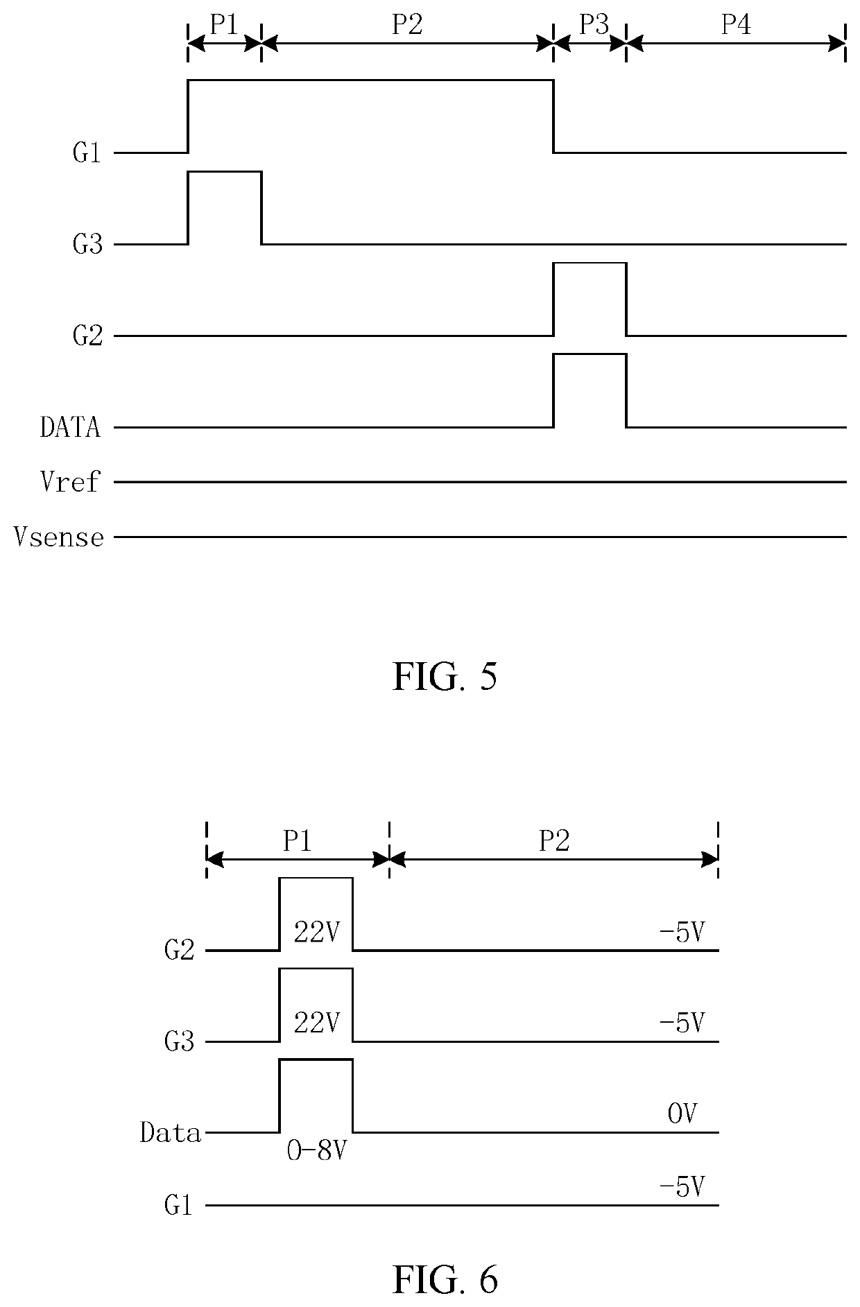
[0046]Referring to FIG. 4, FIG. 4 is a schematic structural diagram of a mixed compensation pixel circuit provided by an embodiment of the present disclosure. The mixed compensation pixel circuit includes an internal compensation circuit 1 and an external compensation circuit 2;

[0047]the internal compensation circuit 1 includes a first thin film transistor T1, a second thin film transistor T2, a third thin film transistor T3, and a fourth thin film transistor T4, a gate of the first thin film transistor T1 is connected to a first node A1, and a source and a drain of the first thin film transistor T1 are respectively connected to a second node B and a DC high voltage power supply VDD, a gate of the second thin film transistor T2 is connected to a third node...


PUM

PropertyMeasurementUnit
reference voltageaaaaaaaaaa
threshold voltageaaaaaaaaaa
relative voltageaaaaaaaaaa

Abstract

The present disclosure provides a mixed compensation pixel circuit, control method, and display device, the mixed compensation pixel circuit includes an internal compensation circuit and an external compensation circuit. The internal compensation circuit includes a first thin film transistor, a second thin film transistor, a third thin transistor, and a fourth thin transistor, the external compensation circuit includes a fifth thin transistor. By optimizing the pixel circuit architecture, the present disclosure does not have an NTFT with a positive long-term relative voltage, improves the stability of the circuit, simplifies the compensation process, and improves the accuracy of compensation.

Description

FIELD OF INVENTION[0001]The present disclosure relates to the field of display technologies, and more particularly to a mixed compensation circuit, a control method thereof, and a display device.BACKGROUND OF INVENTION[0002]Currently, N-type thin film transistors (n-TFT) usually use internal and external mixed compensation pixel circuits as shown in FIG. 1. An internal compensation operation time sequence of the mixed compensation pixel circuit is shown in FIG. 2. As shown in FIG.[0003]2, the operation time sequence includes the following four steps:[0004]P1, resetting step: resetting the gate-source of the driver T1.[0005]P2, acquiring Vth (threshold voltage): inputting Vref (reference voltage) to node N1, and rising a voltage of node N2 to, VN2=Vref−Vth.[0006]P3, inputting data: changing Node N1 from Vref to Vdata (data signal):VN2=(Vdata−Vref)*C1 / (C1+C2)+Vref−Vth.P4, light-emitting: Vgs=Vdata−(Vdata−Vref)*C1 / (C1+C2)−Vref+Vth.[0007]During the light-emitting step, a thin film trans...

Claims


Application Information

Patent Timeline
Patent Type & Authority Applications(United States)
IPC IPC(8): G09G3/3233
CPCG09G3/3233G09G2300/0842G09G2300/0819G09G2300/0852G09G2310/0251G09G2320/0295
Inventor CAI, ZHENFEI
Owner SHENZHEN CHINA STAR OPTOELECTRONICS SEMICON DISPLAY TECH CO LTD
Why Eureka
Try Eureka