DC/DC converter and semiconductor device using DC/DC converter

Active Publication Date: 2008-06-19
SEMICON ENERGY LAB CO LTD
View PDF17 Cites 4 Cited by
  • Summary
  • Abstract
  • Description
  • Claims
  • Application Information

AI Technical Summary

Benefits of technology

[0039]By using a DC/DC converter of the present invention, power that is supplied to another circuit can be stabilized. Thus, operation defects of another circuit can be reduced.
[0040]Further, by manufacturing a semiconductor device using a DC/DC converter of the present invention, power that is supplied from an antenna can be stabilized. Thus, operation defects of another circuit can be reduced. In addition, the response output to the external of the semiconductor device can be prevented from reduction. In other words, the communication distance can be increased. Furthermore, a large amount of power can be used in comparison with the case using power supplied from an antenna; ther

Problems solved by technology

As long as such memory is used, it is di

Method used


Image

  • DC/DC converter and semiconductor device using DC/DC converter
  • DC/DC converter and semiconductor device using DC/DC converter
  • DC/DC converter and semiconductor device using DC/DC converter

Examples


embodiment mode 1

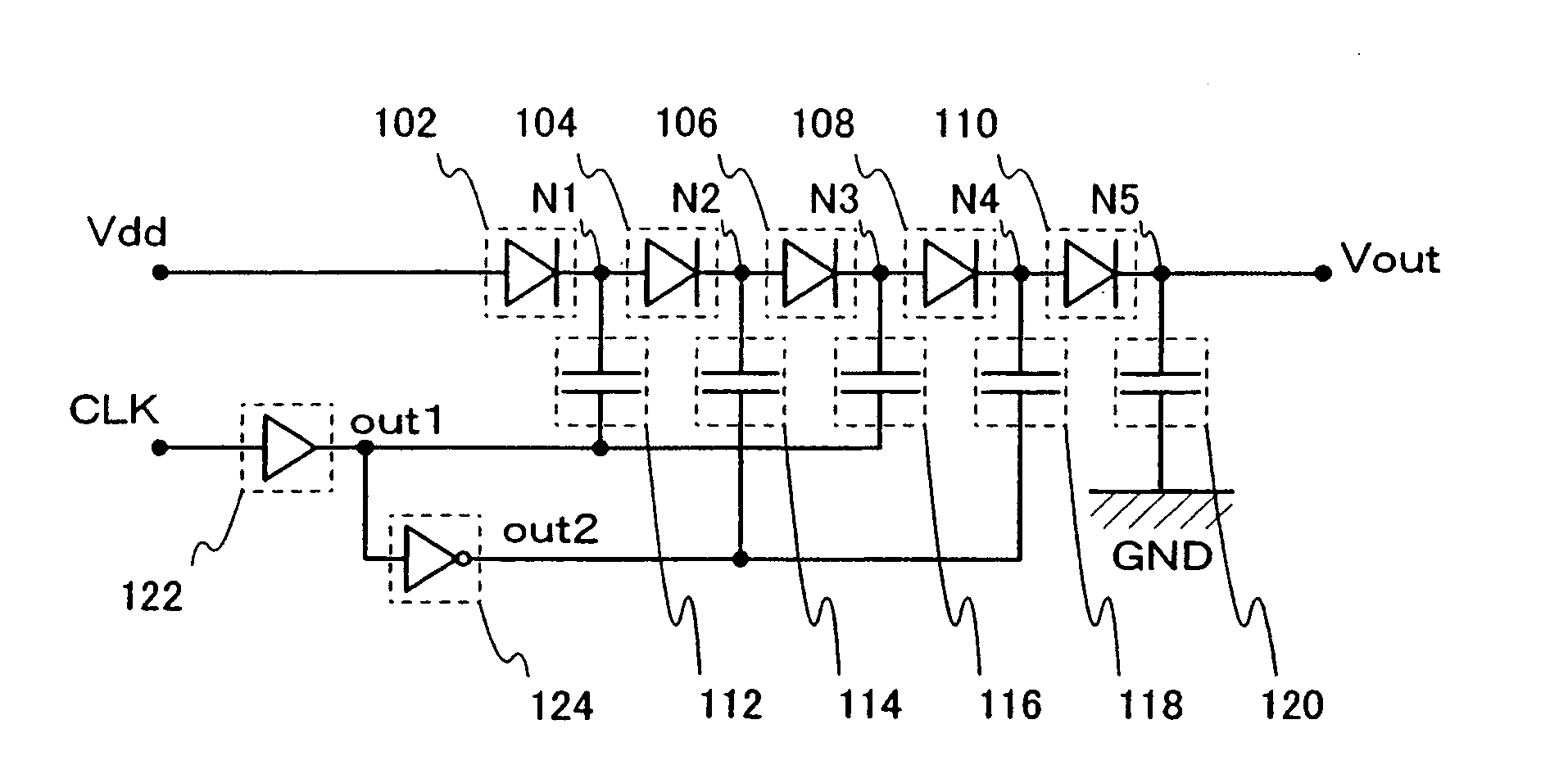
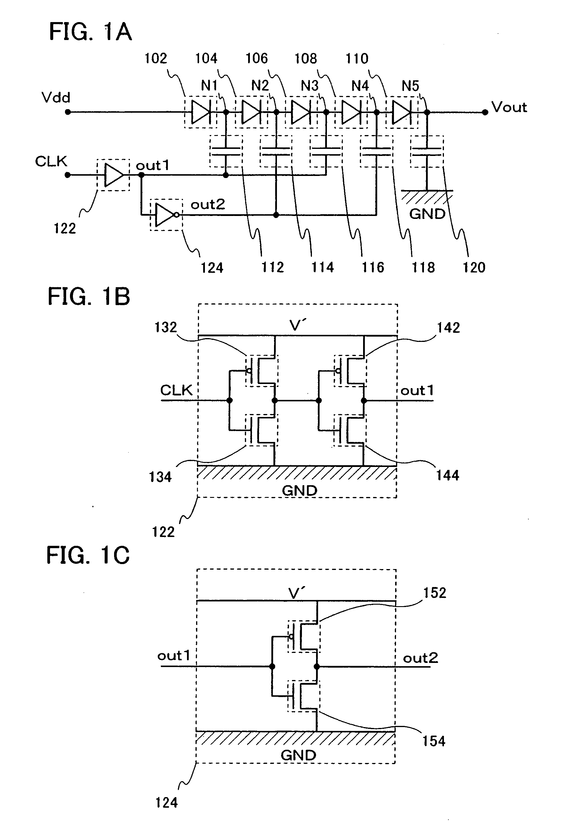
[0061]This embodiment mode will describe a basic structure of a DC / DC converter of the present invention with reference to FIGS. 1A to 1C and FIG. 2.

[0062]FIG. 1A shows an example of a DC / DC converter of the present invention in which boosting of four stages is performed. In FIG. 1A, potential of an input terminal of a first diode 102 is power supply potential Vdd, and an input terminal of a second diode 104 and one of terminals of a first capacitor 112 are connected to an output terminal of the first diode 102. Similarly, an input terminal of a third diode 106 and one of terminals of a second capacitor 114 are connected to an output terminal of the second diode 104. An input terminal of a fourth diode 108 and one of terminals of a third capacitor 116 are connected to an output terminal of the third diode 106. Connections of other parts are similar to the above, and therefore, detailed explanation is omitted. However, the connection can be represented as follows: one of terminals of...

embodiment mode 2

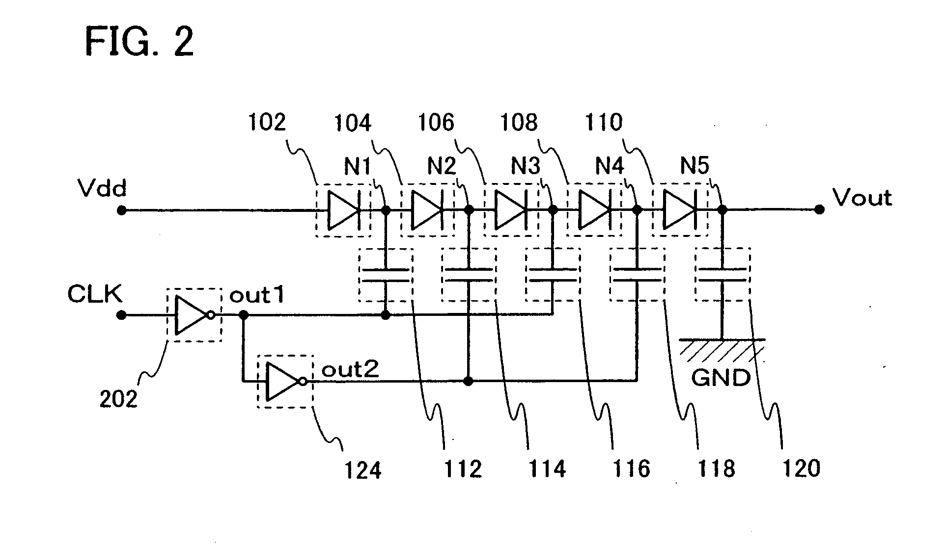
[0075]This embodiment mode will describe a variation of the DC / DC converter shown in Embodiment Mode 1 with reference to FIG. 3.

[0076]FIG. 3 shows another example of a DC / DC converter of the present invention in which boosting of four stages is performed. In FIG. 3, potential of an input terminal of a first diode 302 is power supply potential Vdd, and an input terminal of a second diode 304 and one of terminals of a first capacitor 312 are connected to an output terminal of the first diode 302. Similarly, an input terminal of a third diode 306 and one of terminals of a second capacitor 314 are connected to an output of the second diode 304. Connections of other parts are similar to the above, and therefore, detailed explanation is omitted. However, the connection can be represented as follows: one of terminals of an n-th capacitor is connected to an output of an n-th diode (n: an integer). Further, an input terminal of the n-th diode is connected to an output terminal is an (n−1)-th...

embodiment mode 3

[0084]This embodiment mode will describe a semiconductor device in which a DC / DC converter of the present invention is used with reference to FIGS. 4A to 5B.

[0085]FIG. 4A is an example of a structure of a semiconductor device in which a DC / DC converter of the present invention is used. An antenna 402 is connected to an input terminal of a power supply circuit 404 and an input terminal of a charge circuit 416. An output terminal of the power supply circuit 404 is connected to an input terminal of a constant voltage circuit 406, and an output terminal of the constant voltage circuit 406 is connected to an input terminal of a DC / DC converter 408, a logic circuit 410, and an analog circuit 412. An output terminal of the charge circuit 416 is connected to an input terminal of a secondary battery 418. An output terminal of the secondary battery 418 is connected to the input terminal of the DC / DC converter 408, and an output terminal of the DC / DC converter 408 is connected to a memory circ...


PUM


Abstract

It is an object to provide a DC/DC converter that can stabilize power supply potential in use. It is another object to provide a semiconductor device in which circuit operation is stabilized. In addition to a power supply that supplies potential to be reference potential of boosting in a DC/DC converter, a power supply for charging a capacitor in the DC/DC converter is provided. Accordingly, loads to the power supply that supplies the reference potential of boosting can be reduced. Further, as power for charging the capacitor in the DC/DC converter, power supplied from not an antenna but a secondary battery is used. More specifically, a secondary battery is used as a power supply that supplies power to a buffer circuit or an inverter circuit. Thus, power supplied from the antenna can be stabilized. In other words, operation of a logic circuit and an analog circuit can be stabilized.

Description

BACKGROUND OF THE INVENTION[0001]1. Field of the Invention[0002]The present invention relates to a DC / DC converter (also called as a boosting circuit) and a semiconductor device using the DC / DC converter.[0003]2. Description of the Related Art[0004]In recent years, wireless chips which transmit and receive data wirelessly have been developed actively. The wireless chips which transmit and receive data are called an RFID (Radio Frequency Identification) tag, an RF tag, an RF chip, a wireless tag, a wireless processor, a wireless memory, an IC (Integrated Circuit) tag, an IC label, an electronic tag, an electronic chip, or the like. The wireless chips using a silicon substrate is the mainstream in the wireless chips which has already been put into practice.[0005]The wireless chips which transmit and receive data wirelessly (hereinafter, referred to as RFID tags) generally have a structure in which inside circuits are made to operate by power obtained wirelessly. In the structure, each...

Claims


Application Information

Patent Timeline
IPC IPC(8): G05F3/02H02J1/00
CPCH02M3/073
Inventor ITO, MASAFUMI
Owner SEMICON ENERGY LAB CO LTD
Why Eureka
Try Eureka