Fingerprint sensing module

a fingerprint sensing module and fingerprint technology, applied in the field of optical modules, can solve problems affecting the overall image sensing quality, and achieve the effect of improving the image sensing quality of the fingerprint sensing module and small differences in sensing sensitivity

Active Publication Date: 2022-02-17
AU OPTRONICS CORP
View PDF0 Cites 6 Cited by
  • Summary
  • Abstract
  • Description
  • Claims
  • Application Information

AI Technical Summary

Benefits of technology

[0027]Based on the above, in the fingerprint sensing module according to the embodiment of the disclosure, the first photosensitive pixels and the second photosensitive pixels used to sense the different colored lights have a smaller difference in the sensing sensitivity due to the different sizes of their respective photosensitive regions or the different storage capacitance values. Accordingly, the image sensing quality of the fingerprint sensing module is improved.

Problems solved by technology

Therefore, magnitude of a photocurrent generated by the photosensitive material when irradiated by different colored lights are significantly different, resulting in different photosensitive pixels having the same structural design to have different sensing sensitivity for the different colored lights, which affects the overall image sensing quality.

Method used


Image

  • Fingerprint sensing module
  • Fingerprint sensing module
  • Fingerprint sensing module

Examples


first embodiment

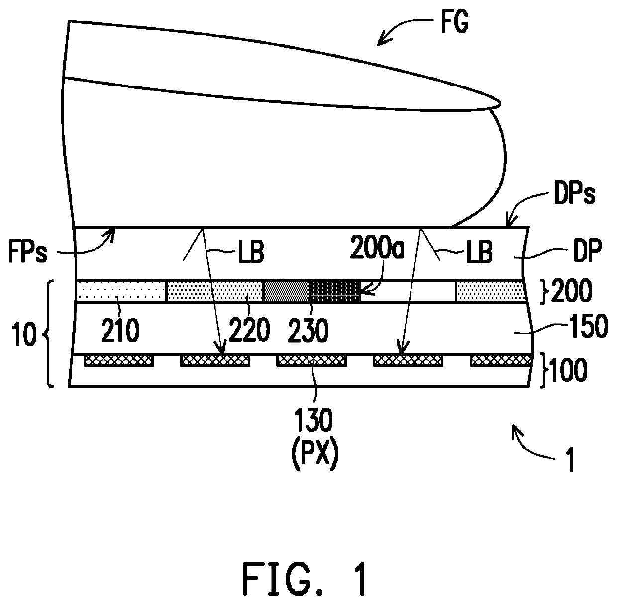
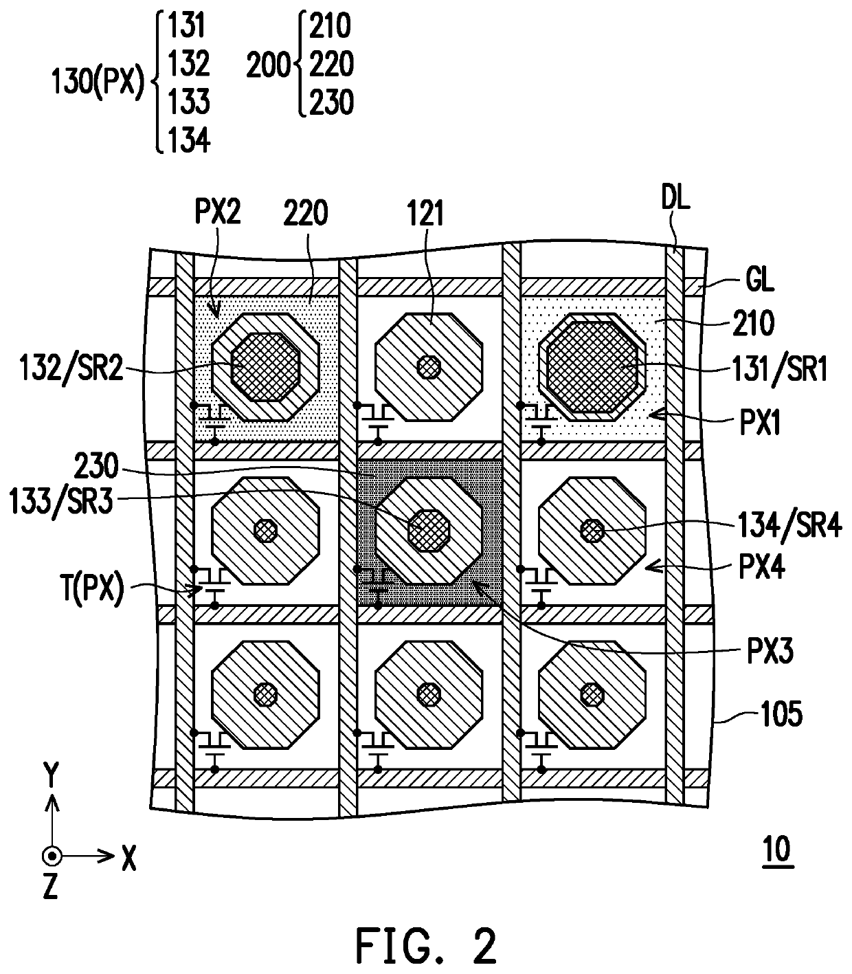
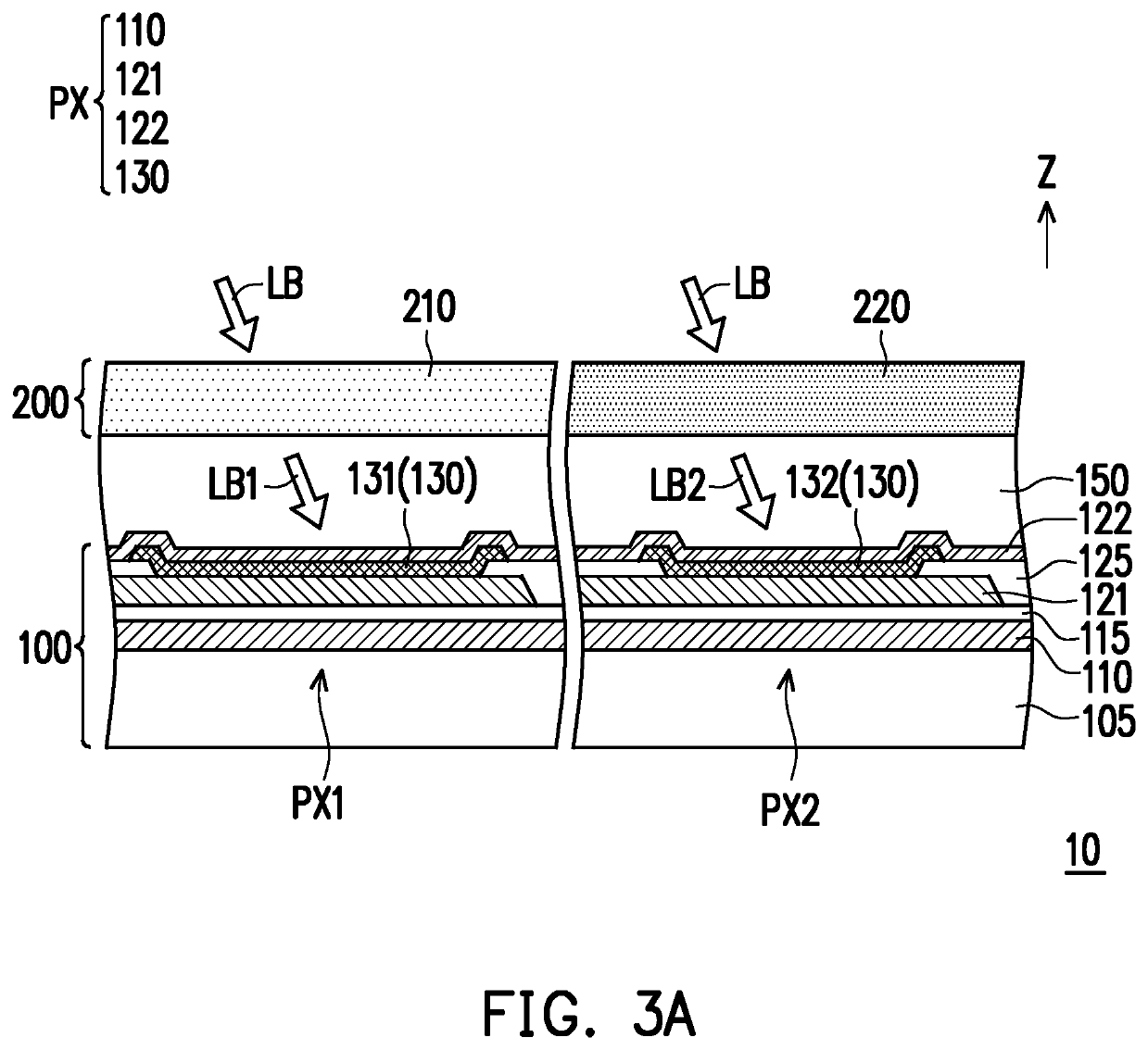
[0048]FIG. 1 is a schematic view of a fingerprint recognition device according to the disclosure. FIG. 2 is a schematic top view of a fingerprint sensing module in FIG. 1. FIGS. 3A and 3B are schematic cross-sectional views of the fingerprint sensing module in FIG. 2. FIG. 4 is a graph of quantum efficiency against wavelength of a photosensitive pattern in FIGS. 3A and 3B. FIG. 5 is a schematic cross-sectional view of the fingerprint sensing module in FIG. 3B with a modification. For clarity of presentation, illustrations of an insulation layer 115, a second electrode 122, and an insulation layer 150 in FIGS. 3A and 3B are omitted in FIG. 2.

[0049]With reference to FIG. 1, a fingerprint recognition device 1 includes a display panel DP and a fingerprint sensing module 10. The fingerprint sensing module 10 is, for example, disposed underneath the display panel DP (that is, on a side of the display panel DP away from a display surface DPs), and the display panel DP is a self-luminous di...

second embodiment

[0064]FIG. 6 is a schematic top view of a fingerprint sensing module according to the disclosure. FIGS. 7A and 7B are schematic cross-sectional views of the fingerprint sensing module in FIG. 6. For clarity of presentation, the illustrations of the insulation layer 115, the second electrode 122, and the insulation layer 150 in FIGS. 7A and 7B are omitted in FIG. 6.

[0065]With reference to FIGS. 6 to 7B, a difference between a fingerprint sensing module 11 of the embodiment and the fingerprint sensing module 10 in FIG. 2 is that the fingerprint sensing module 11 further includes a light shielding pattern layer 140 disposed on the multiple photosensitive patterns 130. In the embodiment, the light shielding pattern layer 140 includes multiple light shielding patterns disposed corresponding to multiple photosensitive pixels PXA, and the light shielding patterns have openings of four different sizes. A material of the light shielding pattern layer 140 may include a metal, a black resin, o...

third embodiment

[0068]FIG. 8 is a schematic top view of a fingerprint sensing module according to the disclosure. With reference to FIG. 8, a difference between a fingerprint sensing module 11A of the embodiment and the fingerprint sensing module 11 in FIG. 6 is that an opening structure of a portion of light shielding patterns of a light shielding pattern layer 140A is different from an opening structure of a portion of the light shielding patterns of the light shielding pattern layer 140. For example, in the embodiment, the light shielding pattern layer 140A defines an opening 142b of a light shielding pattern 142A of a photosensitive region SR2B of a photosensitive pixel PX2B to be composed of multiple separate sub-openings, and the sub-openings of the light shielding pattern 142A are arranged at intervals in the X direction.

[0069]Similarly, the light shielding pattern layer 140A defines an opening 143b of a light shielding pattern 143A of a photosensitive region SR3B of a photosensitive pixel P...


PUM

PropertyMeasurementUnit
quantum efficiencyaaaaaaaaaa
photosensitiveaaaaaaaaaa
quantum efficiencyaaaaaaaaaa

Abstract

A fingerprint sensing module, including a photosensitive element layer and a color filter layer, is provided. The photosensitive element layer has multiple photosensitive regions, and includes a substrate and multiple photosensitive pixels. The photosensitive pixels have multiple photosensitive patterns overlapping the photosensitive regions. The photosensitive pixels include multiple first photosensitive pixels overlapping multiple first photosensitive regions and multiple second photosensitive pixels overlapping multiple second photosensitive regions. A percentage value of a number of the second photosensitive pixels to a number of the photosensitive pixels is less than 30%. An orthographic projection area of each of the first photosensitive regions is different from an orthographic projection area of each of the second photosensitive regions. The color filter layer has multiple openings overlapping the first photosensitive pixels and multiple first color filter patterns overlapping the second photosensitive pixels.

Description

CROSS-REFERENCE TO RELATED APPLICATION[0001]This application claims the priority benefit of Taiwan application serial no. 110112455, filed on Apr. 6, 2021, and the priority benefit of U.S. provisional application. 63 / 066,416, filed on Aug. 17, 2020. The entirety of the abovementioned patent applications are hereby incorporated by reference herein and made a part of this specification.BACKGROUNDTechnical Field[0002]This disclosure relates to an optical module, and in particular to a fingerprint sensing module.Description of Related Art[0003]In order to increase a screen-to-body ratio of a display to realize a narrow bezel design, under-screen fingerprint sensing technology has become a trend. Simply put, the under-screen fingerprint sensing technology is configuring a fingerprint sensing module underneath a display panel of an electronic device. After the electronic device detects that a user touches the display screen, the electronic device controls the display panel to emit light t...

Claims


Application Information

Patent Timeline
Patent Type & Authority Applications(United States)
IPC IPC(8): G06K9/00G02F1/1335G02F1/1333
CPCG06K9/0004G02F1/13338G02F1/133514G02F1/133512G06V40/1318
Inventor CHU, HSUN-CHEN
Owner AU OPTRONICS CORP
Why Eureka
Try Eureka