Nonvolatile memory device and method for producing the same

a non-volatile memory and memory device technology, applied in the direction of semiconductor devices, electrical apparatus, transistors, etc., can solve the problems of reducing the threshold voltage, the data retention characteristic drops, and the threshold voltage drops, so as to reduce the voltage, and improve the data retention characteristic

Inactive Publication Date: 2006-03-30
SONY CORP
View PDF5 Cites 40 Cited by
  • Summary
  • Abstract
  • Description
  • Claims
  • Application Information

AI Technical Summary

Benefits of technology

[0037] According to a nonvolatile memory device of an embodiment of the present invention, an upper limit of the Si—H bond density in the nitride film is defined, and then the charge trap density (or the extinction coefficient at the ultraviolet region of the nitride film) is defined. As a result, the threshold voltage of the memory transistor does not change drastically after retaining the charge at high temperature for a long time. Consequently, there are advantages that the data retention characteristic is good and a difference of the initial threshold voltages can be made small to reduce the voltage.
[0038] According to a nonvolatile memory device of an embodiment of the present invention, a lower limit of the optical bandgap (or an upper limit of the peak wavelength or a lower limit of the peak energy in the luminance spectrum of the nitride film) in the nitride film is defined. As a result, the threshold voltage of the memory transistor does not change drastically after retaining the charge at high temperature for a long time. Consequently, there are advantages that the data retention characteristic is good and a difference of the initial threshold voltages can be made small to reduce the voltage.
[0039] According to a nonvolatile memory device of an embodiment of the present invention, by using a measured result of the extinction coefficient, which is an imaginary number portion of a complex refractive index, which is easier than a measurement of the Si—H bond density, there is an advantage that a determination of a formation condition for defining the Si—H bond density in the nitride film within a predetermined range is performed accurately.
[0040] According to a nonvolatile memory device of an embodiment of the present invention, by using a measured result of the optical bandgap or peak wavelength of the luminance spectrum, there is an advantage that a determination of a formation condition for defining the Si—H bond density in the nitride film within a predetermined range is performed accurately.

Problems solved by technology

Along with the reduction of the voltage in recent days, it is limited to an increase of a difference of the initial threshold voltages.
In the MONOS type nonvolatile memory using the CHE injection described in the above document, or other nonvolatile memories injecting hot carriers into the local area of the nitride film, it suffers from a disadvantage that a retained charge locally dispersed in the vicinity of the drain edge of the nitride film diffuses toward an area without a trapped charge after the retention of long duration at high temperature, and as a result, the threshold voltage drops and the data retention characteristic drops.

Method used


Image

  • Nonvolatile memory device and method for producing the same
  • Nonvolatile memory device and method for producing the same
  • Nonvolatile memory device and method for producing the same

Examples


first embodiment

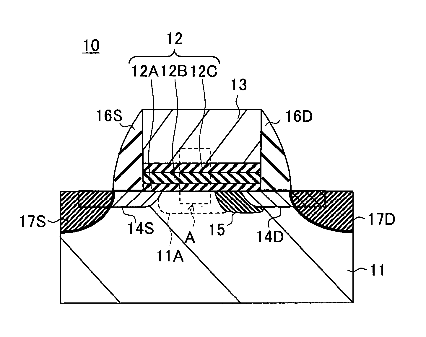
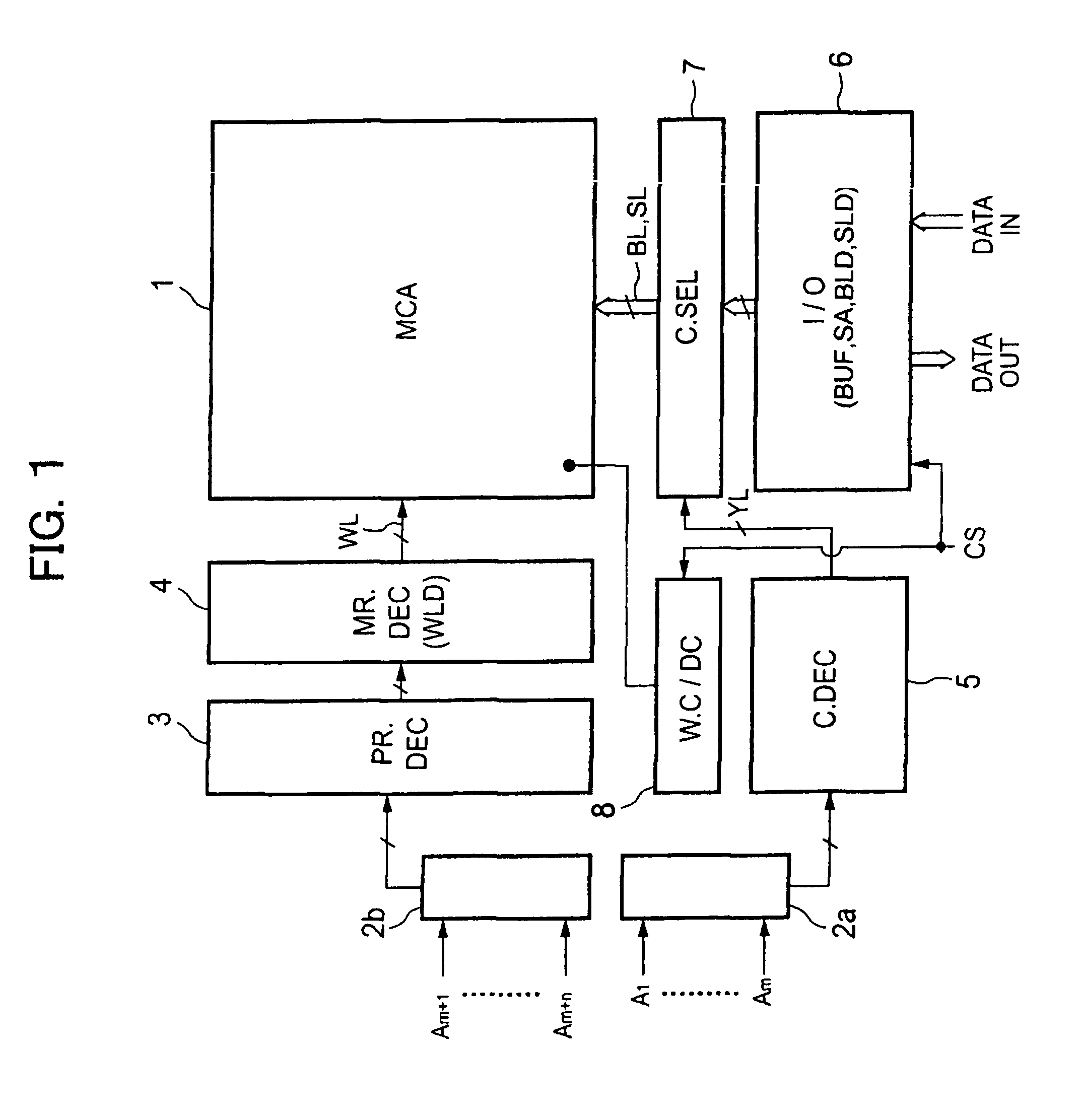
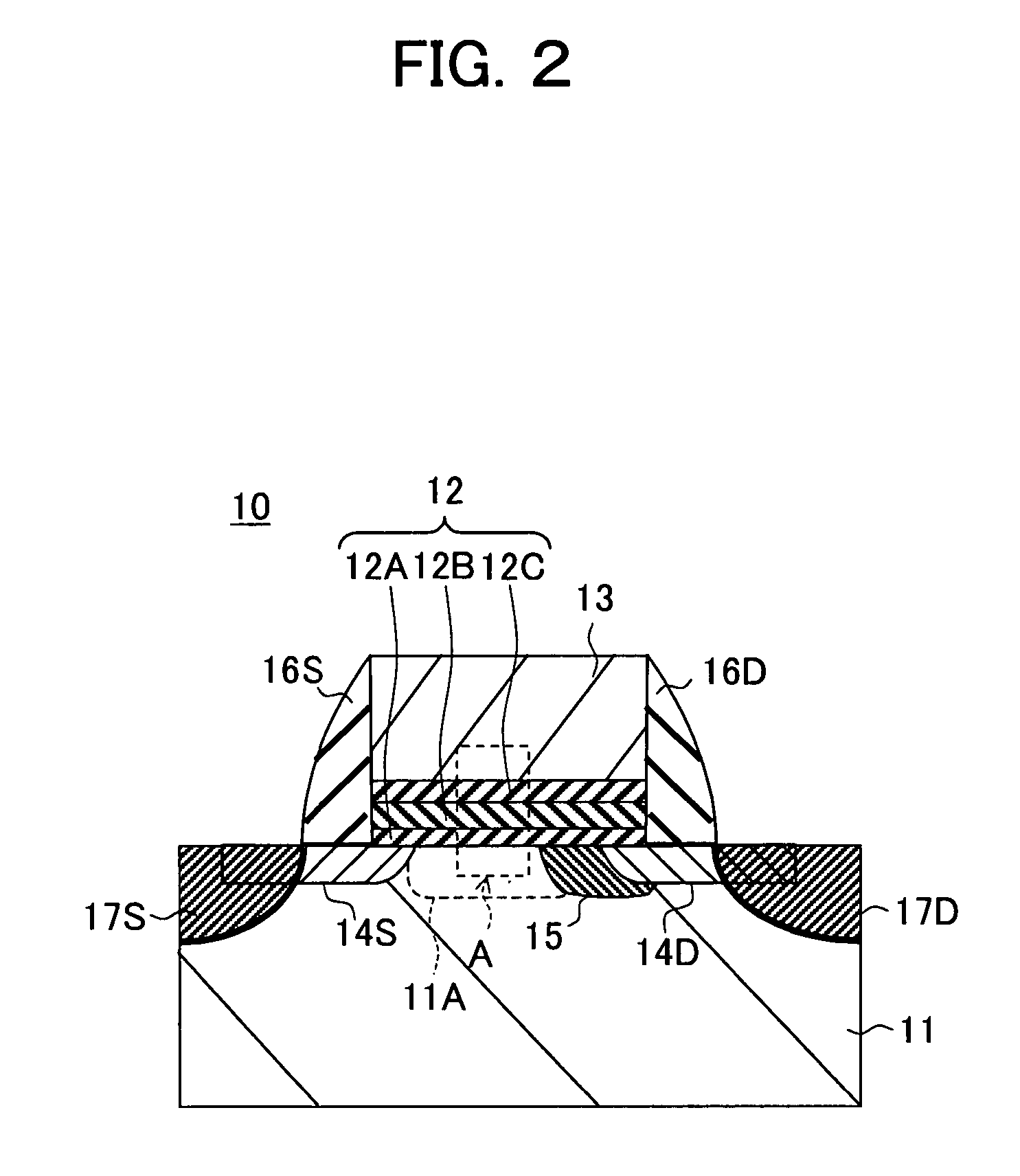
[0067]FIG. 1 is a view of a schematic configuration of a nonvolatile memory device.

[0068] The nonvolatile memory device illustrated in FIG. 1 includes a memory cell array (MCA) 1 having memory transistors arranged in matrix and a memory peripheral circuit for controlling an operation of the memory cell array 1.

[0069] The memory peripheral circuit has a column buffer 2a, a row buffer 2b, a pre-row decoder (PR.DEC) 3, a main-row decoder (MR.DEC) 4, a column decoder (C.DEC) 5, an input and output circuit (I / O) 6, a column selective gate array (C.SEL) 7, and a well charge and discharge circuit (W.C / DC) 8. Note that, in the case of not performing well bias, the well charge and discharge circuit 8 can be omitted. The memory peripheral circuit, not illustrated in the drawing, includes a power source circuit boosting somewhat a power source voltage if necessary and supplying the boosted voltage to the main-row decoder 4 or the well charge and discharge circuit 8, and a control circuit for...

second embodiment

[0128] In the first embodiment, the evaluation of the charge storage layer (nitride film) is performed by using the Si—H bond density, and the measurement is performed by a spectroscopic ellipsometry method.

[0129] In the present embodiment, a higher accuracy evaluation parameter for the charge storage layer (nitride film) will be proposed and a method of evaluating film quality by using the above parameter and a method of producing a nonvolatile memory device including a step of evaluating the film quality will be described.

[0130] Paid attention to that an refractive index changed depending on a composition rate of the nitride film and a boundary portion between the nitride film and the other film could be identified by using a complex refractive index n* (=n+ik), the inventor investigated that the trap density of the nitride film is monitored by using the complex refractive index n* by a detail experimentation.

[0131] As a result, it was learned that the trap density can be monit...

third embodiment

[0159] In the present embodiment, as a parameter of the nitride film for determining the data retention characteristic, a use of an optical bandgap will be proposed instead of the Si—H bond density, the extinction coefficient k, or absorption coefficients α used in the first and the second embodiment. And, a method of evaluating the film quality and a method of producing a nonvolatile memory device including a step of evaluating the film quality will be described.

[0160] The inventor investigated a relationship between the data retention characteristic and an optical property of the nitride film in detail, as a result, obtained an information that an upper limit of an optical bandgap in the nitride film 12B was demanded to suppress the diffusion of the charge injected locally in the nitride film 12B.

[0161] And, the inventor found that, by the optical bandgap given from the absorption coefficients α of the nitride film, defective or indefectible of the data retention characteristic ...


PUM


Abstract

To provide a nonvolatile memory device suppressing a reduction of a data retention characteristic even if charges injected and stored into a local area of a nitride film is redistributed to achieve a reduction of voltage, the nonvolatile memory device in which hot electrons are injected into the local area of the nitride film at one or both of source•drain regions side to store data in a memory transistor is satisfied with a standard for evaluating a film quality of the nitride film, the standard being defined by one of the followings: a density of the bond group of silicon and hydrogen being under 1×1021 cm−3; an extinction coefficient in an ultraviolet region at a wavelength of 240 nm being under 0.10 or the extinction coefficient in 230 nm being under 0.14; an optical energy, a peak wavelength of an luminance spectrum, or a peak energy thereof.

Description

CROSS REFERENCES TO RELATED APPLICATIONS [0001] The present invention contains subject matter related to Japanese Patent Application JP 2004-284037 filed in the Japanese Patent Office on Sep. 29, 2004 and Japanese Patent Application JP 2005-28909 filed in the Japanese Patent Office on Feb. 4, 2005, the entire contents of which being incorporated herein by reference. BACKGROUND OF THE INVENTION [0002] 1. Field of the Invention [0003] The present invention relates to a nonvolatile memory device provided with a metal-oxide-nitride-oxide semiconductor (MONOS) type etc. memory transistor including a nitride film in a plurality of insulation films between a semiconductor region in which a channel is formed and a gate electrode, and injecting hot carriers (high energy charges) into charge traps of a local area in the vicinity of a boundary plane between the nitride film and other insulation film and in a balk layer of the nitride film to store data, and a method of producing the same. [000...

Claims


Application Information

Patent Timeline
Patent Type & Authority Applications(United States)
IPC IPC(8): H01L29/788
CPCH01L21/28282H01L29/792H01L29/66833H01L27/115H01L29/40117H10B69/00
Inventor FUJIWARA, ICHIRO
Owner SONY CORP
Why Eureka
Try Eureka