

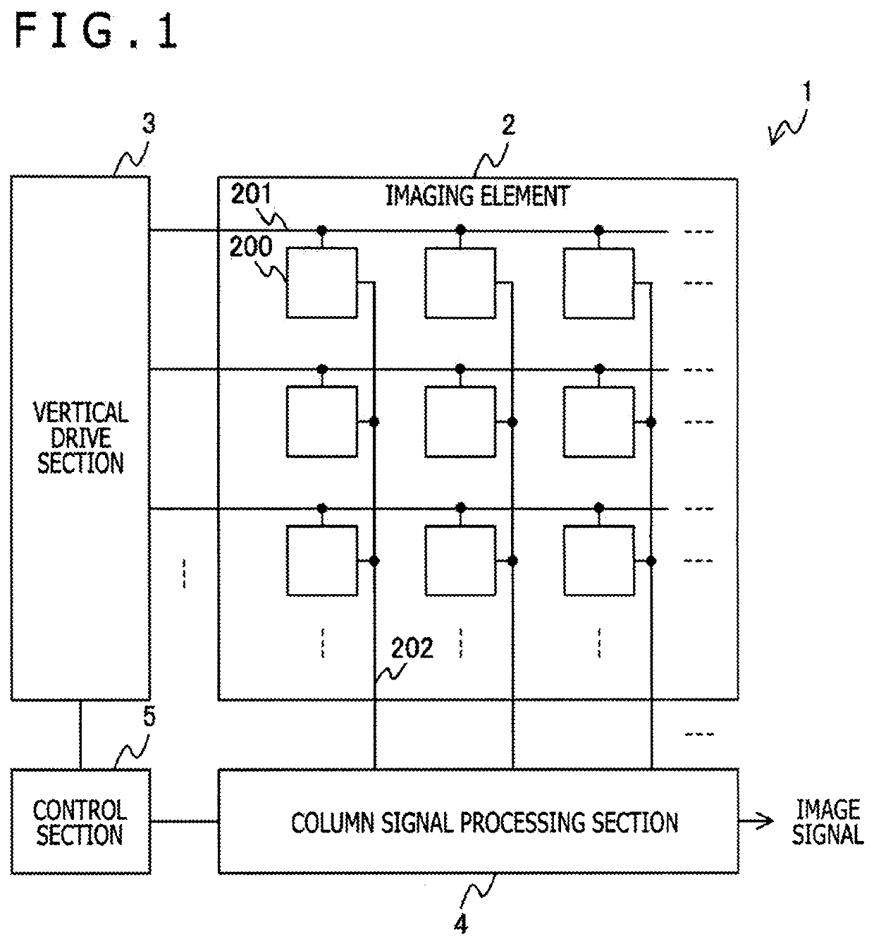
Imaging element and imaging apparatus
a technology which is applied in the field of imaging element and imaging apparatus to achieve the effect of manufacturing imaging elements
- Summary
- Abstract
- Description
- Claims
- Application Information
AI Technical Summary
Benefits of technology
Problems solved by technology
Method used
Image

Examples
second embodiment
2. Second Embodiment
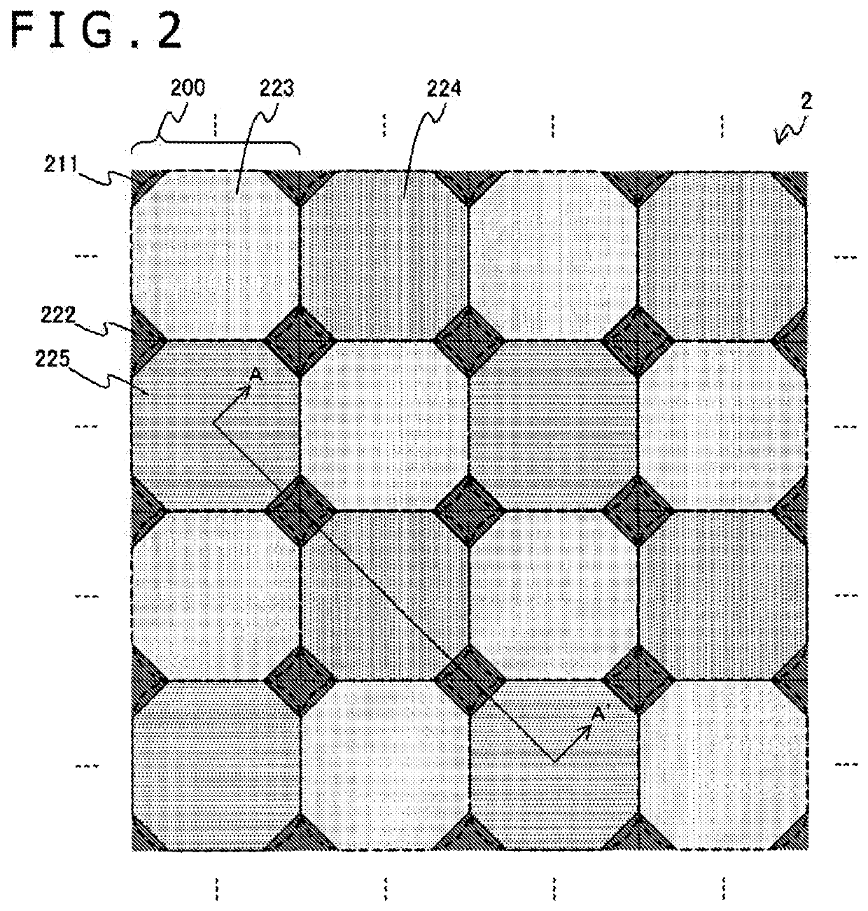
[0056]The imaging element 2 of the first embodiment described above uses the incident light attenuating section 222 which has the quadrilateral shape in light receiving surface view. In contrast to this configuration, an imaging element 2 of a second embodiment, of the present technology is different from the imaging element 2 of the first embodiment in that the imaging element 2 uses a circular incident light attenuating section 222.
[0057][Configuration of Imaging Element]
[0058]FIG. 5 is a view depicting an example of a configuration of the imaging element in the second embodiment of the present technology. The imaging element 2 depicted in the figure is different from the imaging element 2 described with reference to FIG. 2 in that the imaging element 2 of the figure includes an incident light attenuating section 227 instead of the incident light attenuating section 222.
[0059]As represented in the figure, the incident light attenuating section 227 is formed in ...
third embodiment
3. Third Embodiment
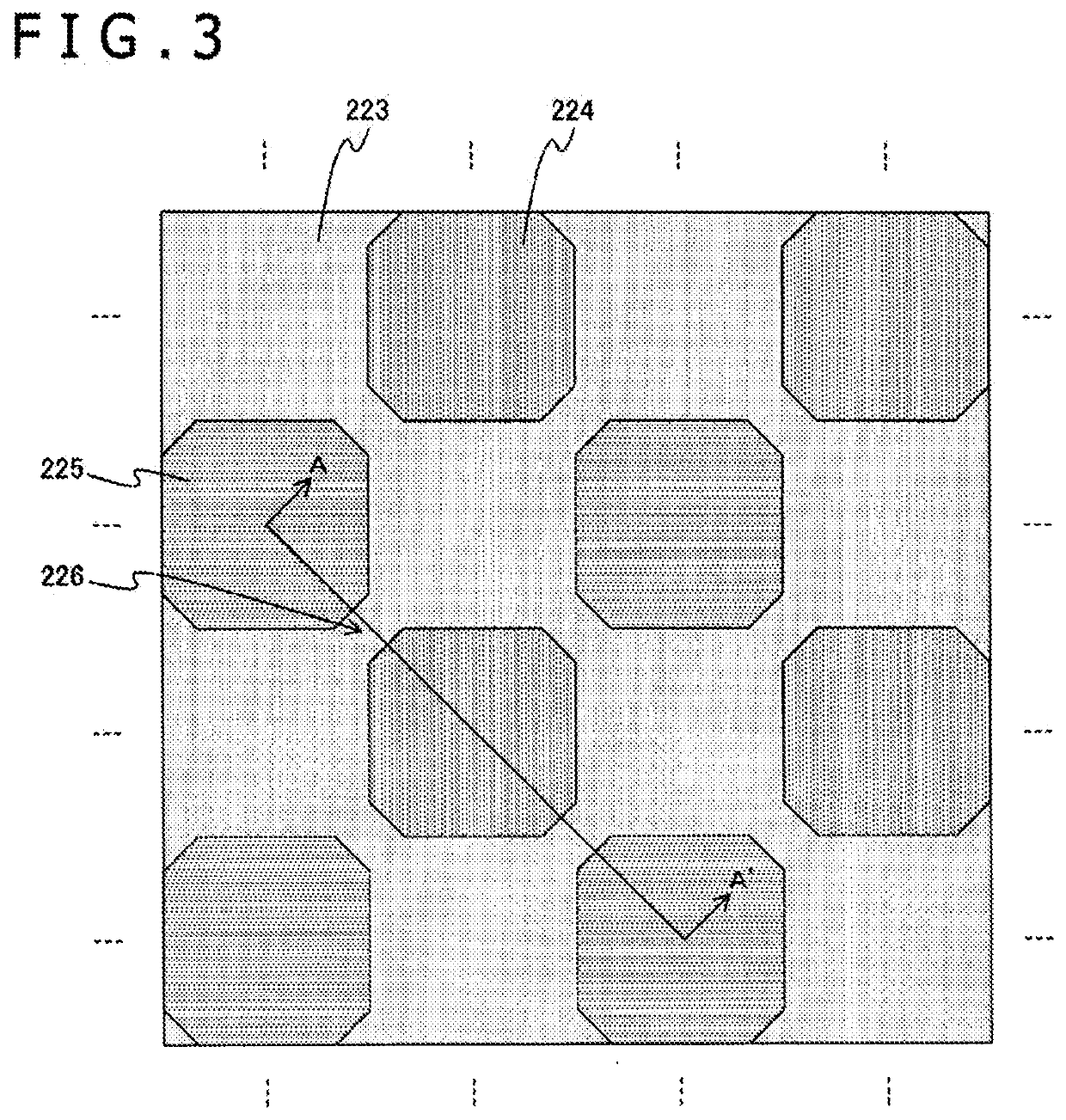
[0062]The incident light attenuating section 222 in the first embodiment described above is arranged in the region of the corners of the adjacent four pixels 200. In contrast to this configuration, as incident light attenuating section of a third embodiment of the present technology is different from the case of the first embodiment in that the incident light attenuating section of the third embodiment is further arranged in adjacent regions in sides of the pixels 200.
[0063][Configuration of Imaging Element]FIG. 6 is a view depicting an example of a configuration of the imaging element in the third embodiment of the present technology. The imaging element 2 depicted in the figure is different from the imaging element 2 described with reference to FIG. 2 in that the imaging element 2 of the figure includes an incident light attenuating section 228 instead of the incident light attenuating section 222.
[0064]The incident light attenuating section 228 of the figure i...
PUM
| Property | Measurement | Unit |
|---|---|---|
| wavelength | aaaaa | aaaaa |
| colors | aaaaa | aaaaa |
| color purity | aaaaa | aaaaa |
Abstract
Description
Claims
Application Information