

SiGeSn LASER DIODES AND METHOD OF FABRICATING SAME
- Summary
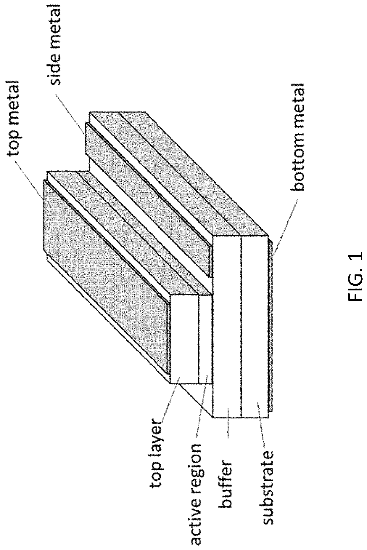
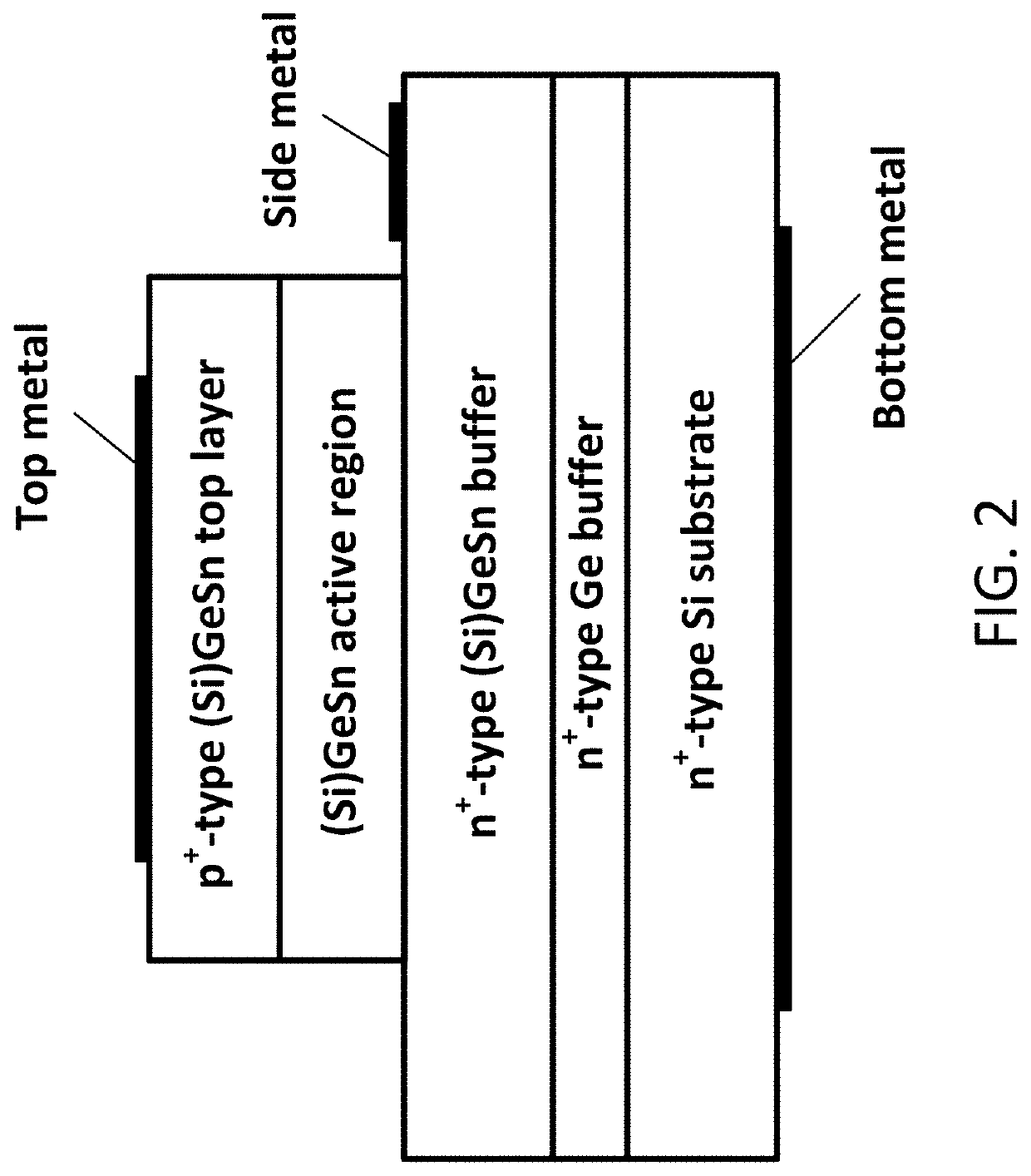
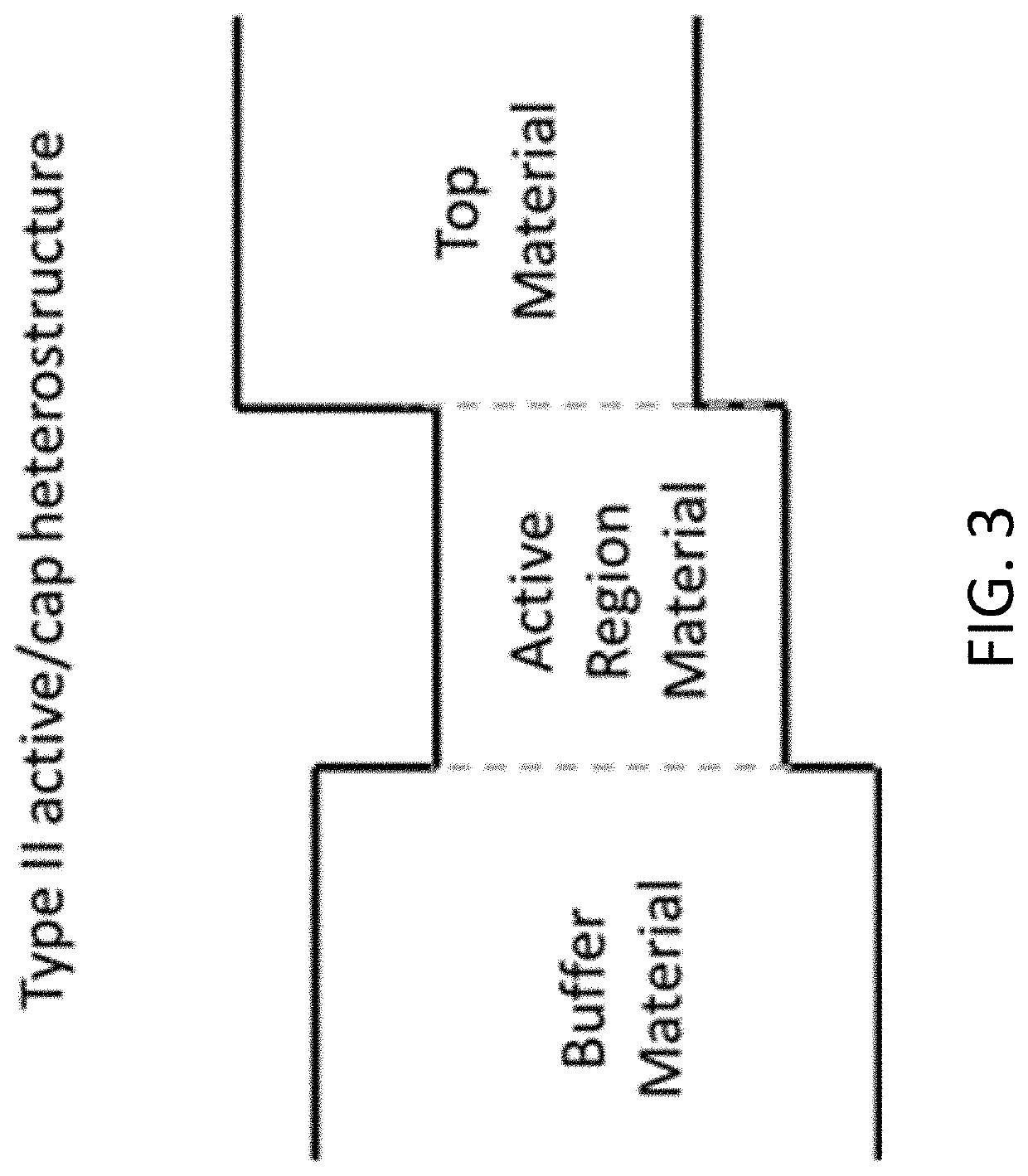
- Abstract
- Description
- Claims
- Application Information
AI Technical Summary
Benefits of technology
Problems solved by technology
Method used
Image

Examples
example
Electrically Injected GeSn Lasers on Si Operating Up to 100 K
[0099]Monolithic lasers on Si have long been anticipated as an enabler of full photonic integration, and significant progress in GeSn material development shows promise for such laser devices. While there are many reports focused on optically pumped lasers, in this exemplary example, the electrically injected GeSn lasers on Si were demonstrated. The GeSn / SiGeSn heterostructure diodes were grown on a Si substrate in a ridge waveguide laser device and tested under pulsed conditions, giving consideration to the structure design to enhance the carrier and optical confinement. The peak linewidth of 0.13 nm (0.06 meV) and injection current curves indicated lasing, which was observed up to 100 K with emission peaks at 2300 nm. The threshold of 598 A / cm2 was recorded at 10 K. The peak power and EQE were measured as 2.7 mW / facet and 0.3%, respectively. The results show major advances for group-IV based lasers, which could serve as ...
PUM
 Abstract
Description
Claims
Application Information