Composite wiring board, package, and electronic device

a technology of composite wiring and electronic devices, applied in the direction of printed circuit non-printed electric components, high frequency circuit adaptations, instruments, etc., can solve the problem of not fully studying the method of stably enhancing the above-described signal path of the flexible substrate used in combination with the terminal substra

Pending Publication Date: 2022-05-12
SUMITOMO METAL SMI ELECTRONICS DEVICES +2
View PDF6 Cites 0 Cited by
  • Summary
  • Abstract
  • Description
  • Claims
  • Application Information

AI Technical Summary

Benefits of technology

[0006]The present invention is made in view of the problem as described above, and has an object to provide a composite wiring board that can stably enhance a bandwidth of a signal path of a flexible substrate electrically joining a signal terminal of a terminal substrate facing a first surface of the flexible substrate and a member facing a second surface of the flexible substrate.
[0012]According to one aspect, a member (typically, a PCB) to be joined to the second signal pad of the flexible substrate faces the second surface, not the first surface, of the flexible substrate, while the signal terminal of the terminal substrate faces the first surface of the flexible substrate. In the composite wiring board, primarily, with a signal path of the flexible substrate being guided to the second surface of the flexible substrate by the first penetration conductive part, adverse influence on characteristic impedance of the signal path due to a configuration near the terminal substrate faced by the first surface can be reduced. Secondarily, with the signal path of the flexible substrate being guided to the first surface of the flexible substrate by the second penetration conductive part, adverse influence on characteristic impedance of the signal path due to a configuration near the member faced by the second surface can be reduced. Based on these advantages, both of the adverse influence on characteristic impedance of the signal path due to the configuration near the terminal substrate faced by the first surface and the adverse influence on characteristic impedance of the signal path due to the configuration near the member faced by the second surface can be reduced. With this configuration, characteristic impedance of the signal path of the flexible substrate can be more easily maintained at a desired value. From the above, it is possible to stably enhance a bandwidth of the signal path of the flexible substrate electrically joining the signal terminal of the terminal substrate facing the first surface of the flexible substrate and the member facing the second surface of the flexible substrate to each other.

Problems solved by technology

A method of stably enhancing a bandwidth of the above-described signal path of the flexible substrate used in combination with the terminal substrate has not yet been fully studied so far.

Method used


Image

  • Composite wiring board, package, and electronic device
  • Composite wiring board, package, and electronic device
  • Composite wiring board, package, and electronic device

Examples


Embodiment Construction

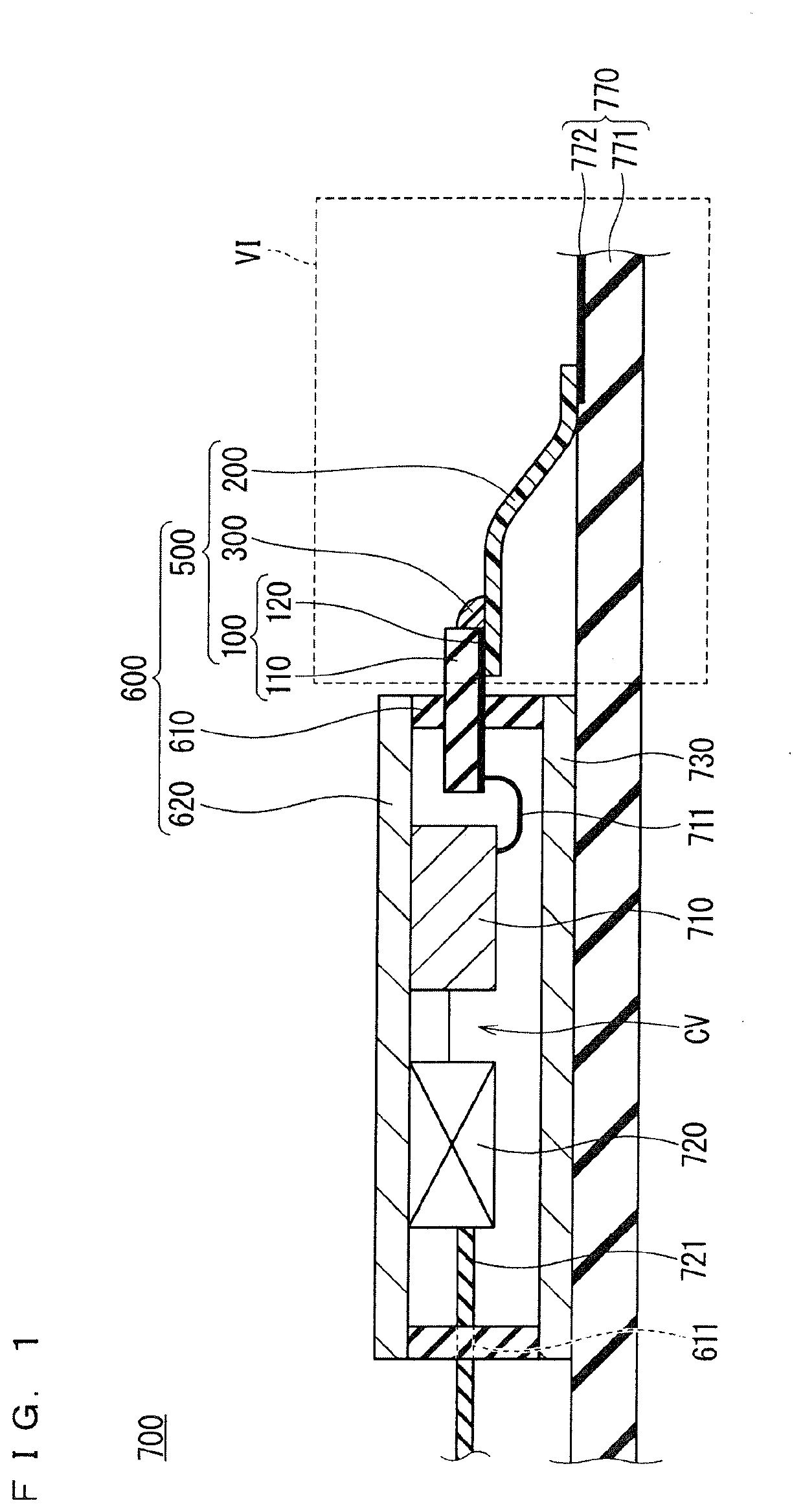
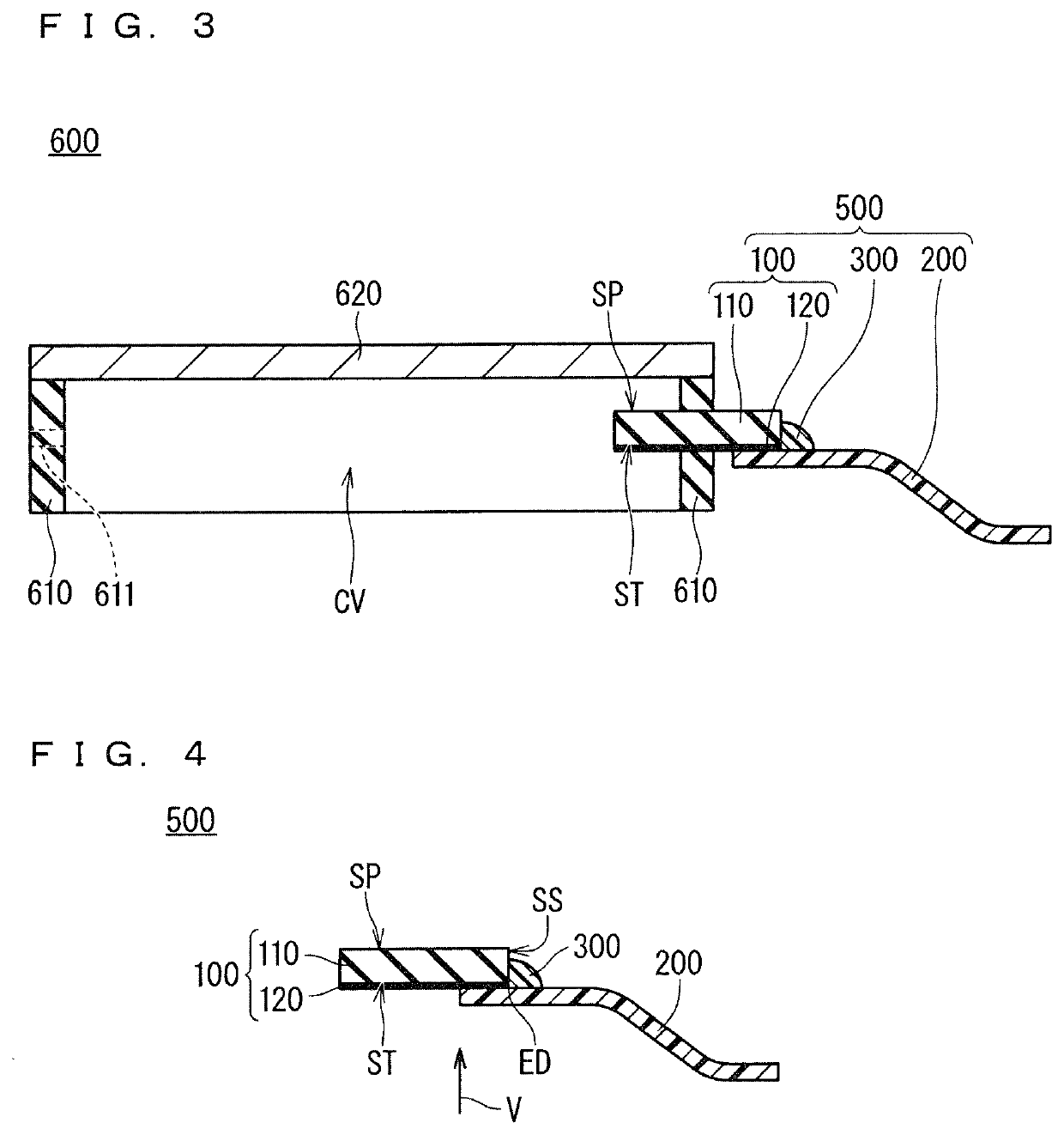
[0028]An embodiment of the present invention will be described below with reference to the drawings. Note that, in the following description, terms related to directions, such as “up”, “down”, “right”, “left”, and “bottom”, are used. Unless otherwise specifically noted, however, these terms are used to distinguish directions, and are not to indicate relation to the gravity direction. Specifically, unless otherwise specifically noted, the orientation of each configuration described in the following description with reference to the gravity direction is arbitrary.

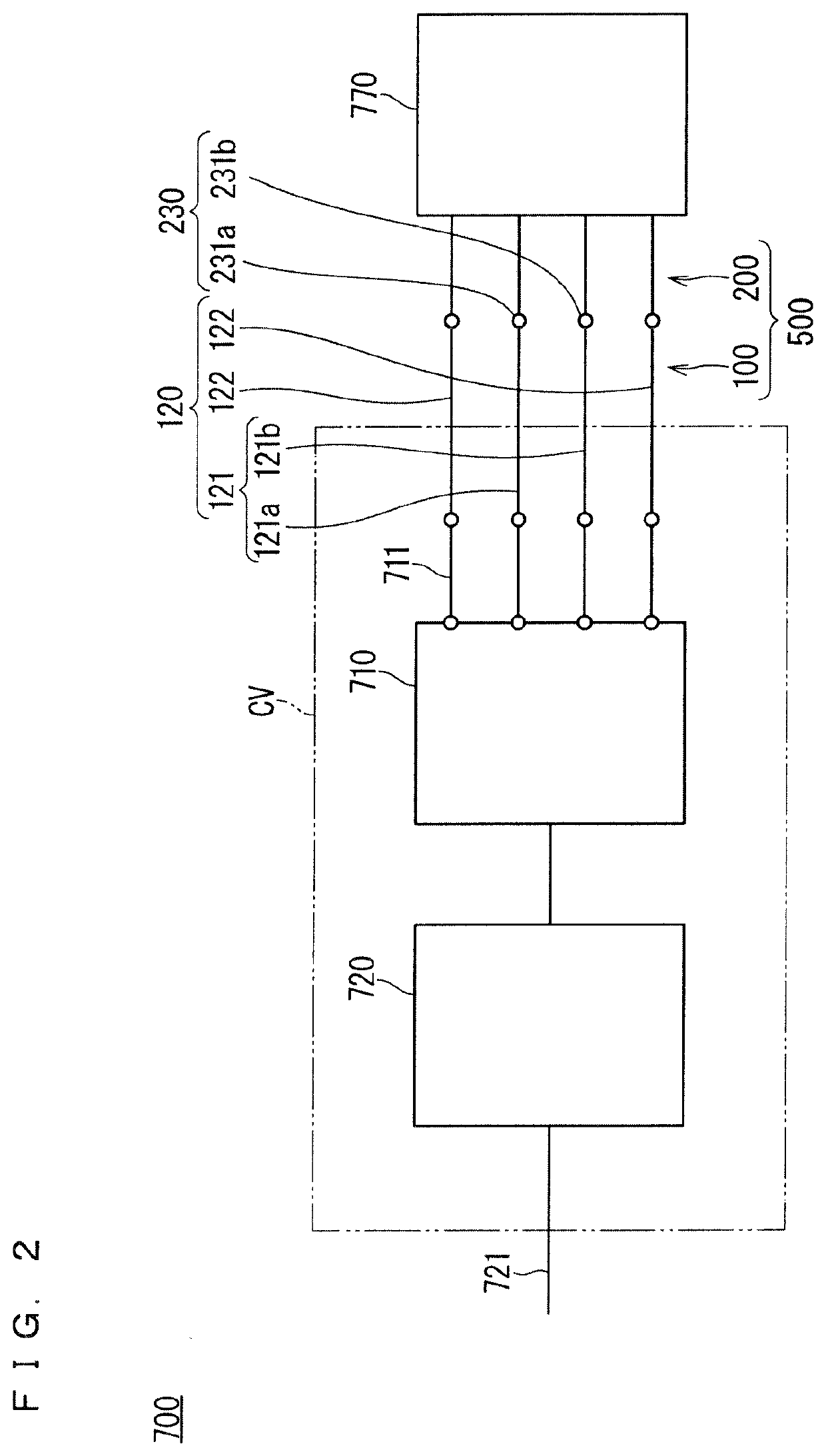
[0029]FIG. 1 and FIG. 2 are a cross-sectional diagram and a block diagram, respectively, schematically illustrating a configuration of an electronic device 700 according to an embodiment. The electronic device 700 includes a package 600 (package with a flexible substrate), an electronic component 710, a bonding wire 711 (electrical connection member), an optical component 720, an optical fiber 721 (light transmission path), a...


PUM

PropertyMeasurementUnit
flexibleaaaaaaaaaa
conductiveaaaaaaaaaa
sizesaaaaaaaaaa

Abstract

A terminal substrate includes a signal terminal disposed on a terminal surface of an insulation ceramic layer. An insulation resin layer of a flexible substrate includes a first surface facing the terminal surface, and a second surface on an opposite side of the first surface. A first signal pad disposed on the first surface is joined to the signal terminal. A first penetration conductive part penetrates the insulation resin layer from the first signal pad. A first signal line is disposed on the second surface. A second penetration conductive part penetrates the insulation resin layer from the first signal line. A second signal line is disposed on the first surface. A third penetration conductive part penetrates the insulation resin layer from the second signal line. A second signal pad is disposed on the second surface.

Description

BACKGROUND OF THE INVENTIONField of the Invention[0001]The present invention relates to a composite wiring board, a package, and an electronic device, and more particularly to a composite wiring board, a package including the composite wiring board, and an electronic device including the package.Description of the Background Art[0002]In recent years, in the field of electronic devices for information communication, enhancing a bandwidth (that is, enhancing communication speed) and downsizing of an apparatus size have been carried out rapidly. At the same time, low loss transmission of high-frequency signals and smaller sizes have been required for packages that accommodate the electronic device for information communication at a high standard. To meet the requirements, a flexible substrate is in some cases used instead of a metal pin, which is widely used as a high-frequency signal transmission path between the package and its outside. The flexible substrate includes an insulation s...

Claims


Application Information

Patent Timeline
Patent Type & Authority Applications(United States)
IPC IPC(8): H05K1/02H05K1/14H05K1/11G02B6/42
CPCH05K1/0245H05K1/148H05K1/118G02B6/4281H05K1/18H05K2201/09236H05K2201/09481H05K2201/09672H05K2201/2018H05K1/0251H05K1/147H05K5/0026H05K3/361H05K1/0306H05K1/0219H05K2201/0154
Inventor KUBO, NOBORUISHIZAKI, MASATOTAKAHASHI, KENTO
Owner SUMITOMO METAL SMI ELECTRONICS DEVICES
Why Eureka
Try Eureka