
Method for Manufacturing Shallow Trench Isolations

a manufacturing method and technology for semiconductor devices, applied in semiconductor/solid-state device manufacturing, basic electric elements, electric devices, etc., can solve the problems of increasing the difficulty of manufacturing semiconductor devices, advancing towards physical possible limits, and difficult to control the trench depth/cd/hm remain loading of storage cell area and peripheral area, etc., to achieve the desired trench depth/cd/hm remain target, the effect of reducing the dislocation d

Pending Publication Date: 2022-06-02
SHANGHAI HUALI MICROELECTRONICS CORP
View PDF4 Cites 0 Cited by
  • Summary
  • Abstract
  • Description
  • Claims
  • Application Information

AI Technical Summary

Benefits of technology

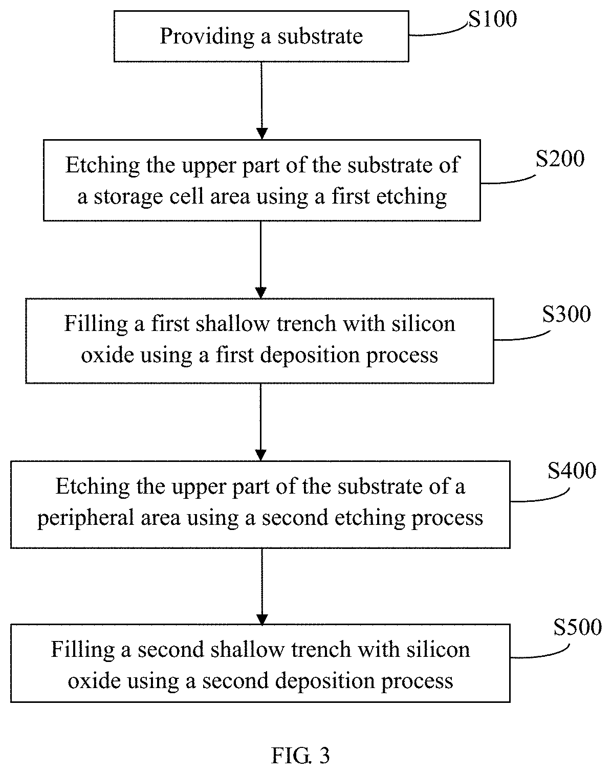
The present invention provides a method for manufacturing shallow trench isolations. This method separately etches trenches in the storage cell area and peripheral area to control the shape of the etched device and improve yield. The shallow trenches are separately filled to eliminate dislocation defects. This results in improved device performance and reliability.

Problems solved by technology

The manufacturing of semiconductor devices has thus become increasingly challenging and advanced towards physically possible limits.
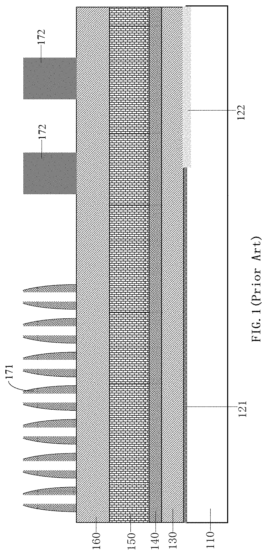
Under the requirements of these process parameters, it is difficult to control the trench depth / CD / HM remain loading of the storage cell area and the peripheral area, and it is relatively difficult to achieve the trench depth / CD / HM remain target required by the device performance of the storage cell area and the peripheral area after final etch.
Meanwhile, the PSZ material filled in a shallow trench isolation trench (STI trench) will cause a dislocation defect of silicon in the peripheral area due to the stress effect.
1) Excessive etching time results in shape damage of the top floating gate structure in the storage cell area and loss of oxide as a protective layer at the top of the floating gate structure;
2) If etching parameters of a high selection ratio of oxide (the material of the gate dielectric layer) to silicon are selected, the taper of the top of the storage cell area STI is not conducive to the formation of a vertical trench shape of the storage cell area STI;
3) If etching parameters of a low selection ratio of oxide (the material of the gate dielectric layer) to silicon are selected, a vertical shape can be easily formed at the top of the STI, but the shape damage of the floating gate layer above the STI and the loss of oxide at the top are exacerbated;
4) Excessive etching results in a depth difference of trenches in the large open area of the peripheral device and the small open area of the storage cell, which is not conducive to last depth control of trenches of STI in different areas.

Method used


Image

  • Method for Manufacturing Shallow Trench Isolations
  • Method for Manufacturing Shallow Trench Isolations
  • Method for Manufacturing Shallow Trench Isolations

Examples


Embodiment Construction

[0083]The following description is provided so that those skilled in the art can implement and use the present invention and combine it into a specific application background. Various modifications, and various uses in different applications will be readily apparent to those skilled in the art, and the general principles defined herein can be applied to a wide range of embodiments. Thus, the present invention is not limited to the embodiments given herein, but should be granted in the broadest scope of the principles and novel features disclosed herein.

[0084]Many specific details are set forth in the following detailed description to provide a thorough understanding of the present invention. However, it would be apparent to those skilled in the art that the practice of the present invention is not necessarily limited to these specific details. In other words, the well-known structures and devices are shown in the form of block diagrams without details to avoid obscuring the present ...


PUM

PropertyMeasurementUnit
temperatureaaaaaaaaaa
reaction temperatureaaaaaaaaaa
thicknessaaaaaaaaaa

Abstract

The disclosure provides a method for manufacturing shallow trench isolations, providing a substrate comprising a storage cell area and a peripheral area of a storage device; etching the upper part of the substrate of the storage cell area using a first etching process to form a first shallow trench, and filling the first shallow trench with silicon oxide using a first deposition process; and etching the upper part of the substrate of the peripheral area using a second etching process to form a second shallow trench, and filling the second shallow trench with silicon oxide using a second deposition process; wherein the depth and characteristic dimension of the first shallow trench are smaller than the depth and characteristic dimension of the second shallow trench. The disclosure can avoid the silicon dislocation defect of the peripheral area and ensure the device shape and characteristic dimension of the storage cell area.

Description

CROSS-REFERENCES TO RELATED APPLICATIONS[0001]This application claims priority to Chinese patent application No. 202011377953.1, filed on Nov. 30, 2020, the disclosure of which is incorporated herein by reference in its entirety.TECHNICAL FIELD[0002]The present invention relates to the field of manufacturing of semiconductor devices, in particular to a method for manufacturing shallow trench isolations of a storage device.BACKGROUND[0003]Since doctor Jack Kilby of Texas Instruments invented an integrated circuit in the early days, scientists and engineers have made many inventions and improvements on semiconductor devices and processes. In the past 50 years, the sizes of semiconductors have been significantly reduced, which has led to a growing processing speed and continuously reduced power consumption. So far, the development of semiconductors roughly follows the Moore's law. The Moore's law generally refers to doubling of the number of transistors in integrated circuits about eve...

Claims


Application Information

Patent Timeline
Patent Type & Authority Applications(United States)
IPC IPC(8): H01L21/762H01L21/308H01L21/3213H10B41/35H10B41/41H10B41/42
CPCH01L21/76224H01L21/32139H01L21/3088H01L21/3086H01L21/76229H10B41/35H10B41/42H10B41/41
Inventor LIU, LIYUANHE, LIQIAO, FULONGWANG, YI
Owner SHANGHAI HUALI MICROELECTRONICS CORP
Learn More