Substrate for flip-chip LED chip, epitaxial wafer and manufacturing method thereof
A technology of LED chip and manufacturing method, which is applied in the direction of electrical components, circuits, semiconductor devices, etc., can solve the problems that the quantum efficiency in the LED chip cannot be fully exerted, the light output efficiency is reduced, and the light cannot be emitted, so as to improve the external quantum efficiency and improve Internal quantum efficiency, the effect of increasing transmission
- Summary
- Abstract
- Description
- Claims
- Application Information
AI Technical Summary
Problems solved by technology
Method used
Image
Examples
Embodiment 1
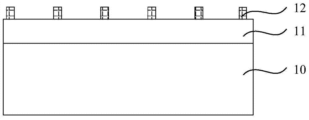
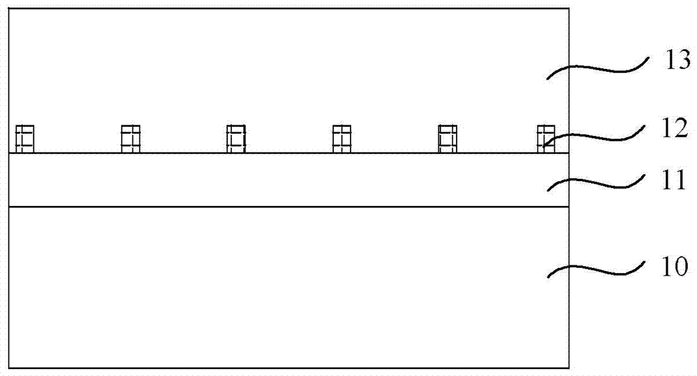
[0052] Such as Figure 7 As shown, this embodiment provides a substrate for flip-chip LED chips, including a gallium nitride substrate material 13 and a dielectric layer 12 with a patterned structure, and the dielectric layer 12 with a patterned structure is embedded in nitrogen GaN substrate material 13.
[0053] Preferably, the patterned structure is a columnar structure arranged at intervals, further, the patterned structure is a columnar structure 12a arranged periodically. Since the sides of the columnar structure are perpendicular to the surface of the substrate, the columnar structure does not have scattering or diffuse reflection. The light reflection of the substrate increases its transmission and improves the light extraction efficiency of the flip-chip LED chip, that is, increases the external quantum efficiency.
[0054] Such as Figure 6 As shown, the substrate for flip-chip LED chips may also include a lattice matching layer 11 located on the surface of the ga...
Embodiment 2
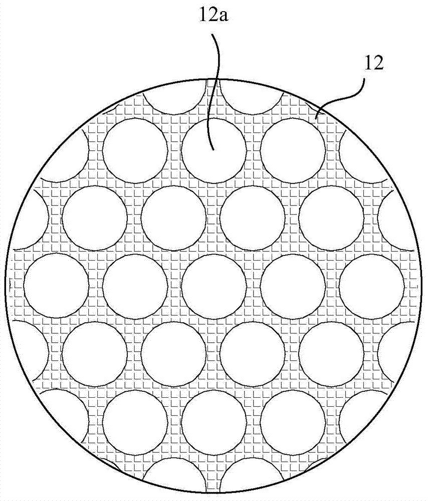
[0069] Figure 8 It is a cross-sectional view of forming a lattice matching layer and a dielectric layer on a sapphire substrate in Embodiment 2 of the present invention, Figure 9 It is a top view of the second lattice matching layer and the dielectric layer in the embodiment of the present invention.
[0070] Such as Figure 8 and Figure 9 As shown, the difference between this embodiment and Embodiment 1 is that the columnar structure 12a is a columnar protrusion, and the dielectric layer 12 is composed of periodically arranged columnar protrusions, and the lattice is exposed through the gaps between the columnar protrusions. The matching layer 11, the gallium nitride substrate material 13 fills the gaps between the columnar protrusions. More specifically, the columnar structure 12a is a cylindrical protrusion. Of course, since the sapphire substrate 10 is a circular substrate, the columnar structures 12a on the edge of the sapphire substrate 10 may be incomplete cylind...
Embodiment 3
[0072] The difference between this embodiment and the first embodiment is that the columnar structure 12a is a polygonal columnar protrusion. Figure 10 It is a top view of the triple lattice matching layer and the dielectric layer according to the embodiment of the present invention. Such as Figure 10 As shown, in this embodiment, the columnar structure 12a is a hexagonal prism protrusion, the lattice matching layer 11 is exposed through the gap between the hexagonal prism protrusions, and the gallium nitride substrate material 13 is filled with Fill the spaces between the hexagonal prism-shaped protrusions.
PUM
| Property | Measurement | Unit |
|---|---|---|
| thickness | aaaaa | aaaaa |
| thickness | aaaaa | aaaaa |
Abstract
Description
Claims
Application Information
 - R&D
- Intellectual Property
- Life Sciences
- Materials
- Tech Scout
- Unparalleled Data Quality
- Higher Quality Content
- 60% Fewer Hallucinations
Browse by: Latest US Patents, China's latest patents, Technical Efficacy Thesaurus, Application Domain, Technology Topic, Popular Technical Reports.
© 2025 PatSnap. All rights reserved.Legal|Privacy policy|Modern Slavery Act Transparency Statement|Sitemap|About US| Contact US: help@patsnap.com


