Two-dimensional material flexible substrate structure, focal plane optical detector array and manufacturing method thereof

A flexible substrate, two-dimensional material technology, used in semiconductor devices, climate sustainability, final product manufacturing, etc., can solve lattice mismatch, flexible substrates cannot fully absorb and release stress, and cannot meet absolute flexibility and other problems, to achieve the effect of large absolute flexibility, increase device integration function, and reduce device dark current

Inactive Publication Date: 2018-06-12
CHAOJING TECH BEIJING CO LTD
View PDF6 Cites 3 Cited by
  • Summary
  • Abstract
  • Description
  • Claims
  • Application Information

AI Technical Summary

Problems solved by technology

[0008] In view of the shortcomings of the prior art described above, the purpose of the present invention is to provide a two-dimensional material flexible substrate structure, focal plane photodetector array and manufacturing method, which are used to solve the problem of large area array photodetection in the prior art. The bottleneck of epitaxial growth technology is lattice mismatch, and the flexible substrate prepared by conventional methods cannot completely absorb and release stress, and cannot meet the problem of absolute flexibility.

Method used


Image

  • Two-dimensional material flexible substrate structure, focal plane optical detector array and manufacturing method thereof
  • Two-dimensional material flexible substrate structure, focal plane optical detector array and manufacturing method thereof
  • Two-dimensional material flexible substrate structure, focal plane optical detector array and manufacturing method thereof

Examples


Embodiment 1

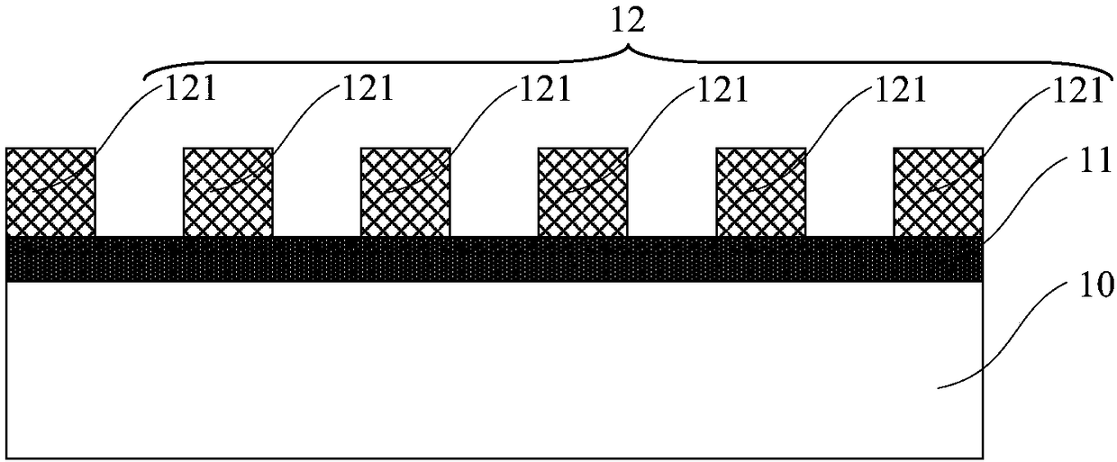
[0075] see figure 1 , the present invention provides a two-dimensional material flexible substrate structure, the two-dimensional material flexible substrate structure includes: a supporting substrate 10; a two-dimensional material layer 11, the two-dimensional material layer 11 is located on the supporting substrate 10 surface; a patterned flexible substrate 12, the patterned flexible substrate 12 is located on the surface of the two-dimensional material layer 11; the patterned flexible substrate 12 includes several pattern units 121 distributed at intervals. The two-dimensional material flexible substrate structure of the present invention combines the patterned flexible substrate 12 with the two-dimensional material layer 11, and the interface between the patterned flexible substrate 12 and the two-dimensional material layer 11 The van der Waals bond greatly weakens the attraction between the upper and lower atoms, and the strength of the van der Waals force formed at the ...

Embodiment 2

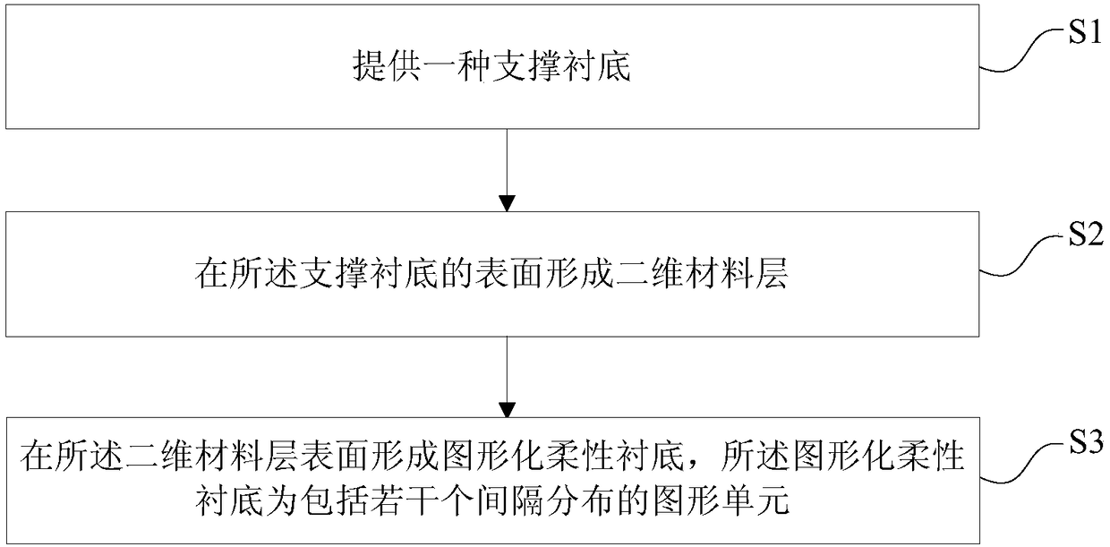
[0084] see figure 2 , the present invention also provides a method for manufacturing a two-dimensional material flexible substrate structure, the method for manufacturing a two-dimensional material flexible substrate structure includes the following steps:

[0085] 1) providing a support substrate;

[0086] 2) forming a two-dimensional material layer on the surface of the supporting substrate;

[0087] 3) A patterned flexible substrate is formed on the surface of the two-dimensional material layer, and the patterned flexible substrate includes several pattern units distributed at intervals.

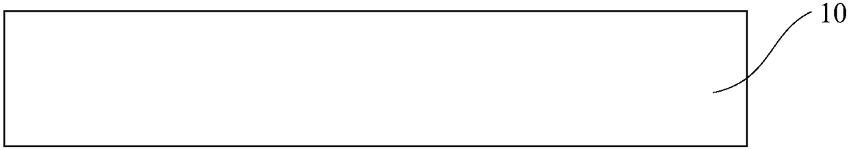
[0088] To perform step 1), see figure 2 Step S1 in and image 3 , providing a support substrate 10 .

[0089] As an example, the supporting substrate 10 may be a semiconductor substrate, a semi-insulator substrate, an insulator substrate, a thermally conductive material substrate or a metal substrate. Preferably, in this embodiment, the supporting substrate 10 is a Si substrate.

...

Embodiment 3

[0112] see Figure 15 , the present invention also provides a focal plane photodetector array, the focal plane photodetector array includes: the two-dimensional material flexible substrate structure as described in Embodiment 1, the two-dimensional material flexible substrate structure Please refer to Embodiment 1 for the specific structure, which is no longer similar here; the photodetector structure 17, the photodetector structure 17 is located on the surface of each pattern unit 121 in the patterned substrate 12, that is, the photodetector structure 17 is a structure distributed in a periodic array.

[0113] As an example, the photodetector structure 17 may be, but not limited to, include In 0.82 Ga 0.18 2.5 µm photodetector structure with As absorbing layer.

[0114] As an example, the photodetector structure 17 may be a structure of upper and lower electrodes, or a structure of coplanar electrodes.

[0115] As an example, the focal plane photodetector array further in...


PUM


Abstract

The invention provides a two-dimensional material flexible substrate structure, a focal plane optical detector array and a manufacturing method thereof. The two-dimensional material flexible substratestructure comprises a support substrate, a two-dimensional material layer positioned on the surface of the support substrate, and a patterned flexible substrate positioned on the surface of the two-dimensional material layer. The patterned flexible substrate comprises a plurality of pattern units spaced at intervals. According to the two-dimensional material flexible substrate structure providedby the invention, the patterned flexible substrate is combined with the two-dimensional material layer, attraction between upper and lower atoms is greatly weakened by Van der Waals bonding at an interface between the patterned flexible substrate and the two-dimensional material, strength of a Van der Waals force formed at the interface is far less than bond energy of a covalent bond, and the patterned flexible substrate can completely self-control strain absorption and release stress, eliminate or reduce threading dislocation and other lattice structural defects to the greatest extent, and has extremely high absolute flexibility.

Description

technical field [0001] The invention belongs to the technical field of semiconductors, and relates to a two-dimensional material flexible substrate structure, a focal plane photodetector array and a manufacturing method. Background technique [0002] The short-wave infrared (SWIR, 1-3 micron) InGaAs focal plane detector array can meet the application requirements of "all-day, multi-weather". Civilian fields such as safety inspection, fire prevention warning, industrial inspection and driving vision enhancement have extensive and important application value1-3. InGaAs material has high quantum efficiency, good material stability, and can work at room temperature. The device performance of the same short-wave infrared band exceeds that of mercury cadmium telluride devices. The InGaAs detector has high imaging contrast, clear target details, and high recognition in target recognition. Due to the perfect match between the InGaAs absorption spectrum and the radiance band of the...

Claims


Application Information

Patent Timeline
Patent Type & Authority Applications(China)
IPC IPC(8): H01L31/0236H01L31/09H01L31/18
CPCH01L31/02366H01L31/09H01L31/1844H01L31/1852Y02P70/50
Inventor 王庶民
Owner CHAOJING TECH BEIJING CO LTD
Why Eureka
Try Eureka