Substrate and epitaxial wafer for flip LED chips and making methods thereof

A technology of LED chip and manufacturing method, which is applied in the direction of electrical components, circuits, semiconductor devices, etc., can solve the problems of reducing light extraction efficiency, light cannot be emitted, and the quantum efficiency in the LED chip cannot be fully exerted, so as to improve the external quantum efficiency and increase Effect of transmission and improvement of internal quantum efficiency

Active Publication Date: 2015-08-12
HANGZHOU SILAN AZURE
View PDF7 Cites 7 Cited by
  • Summary
  • Abstract
  • Description
  • Claims
  • Application Information

AI Technical Summary

Problems solved by technology

However, the inventors found that the flip-chip LED chip structure emits light on the N surface. Since the refractive index of sapphire is lower than that of gallium nitride, the light emitted from the epitaxial layer will be reflected on the interface between the sapphire and the substrate. As a result, more light cannot be emitted, especially the patterned substrate currently used in the mainstream LED chip structure has scattering and diffuse reflection effects, which is more likely to cause more light not to be emitted, reducing the light extraction efficiency; but if Without the use of patterned substrate technology, the internal quantum efficiency of LED chips cannot be fully utilized

Method used


Image

  • Substrate and epitaxial wafer for flip LED chips and making methods thereof
  • Substrate and epitaxial wafer for flip LED chips and making methods thereof
  • Substrate and epitaxial wafer for flip LED chips and making methods thereof

Examples


Embodiment 1

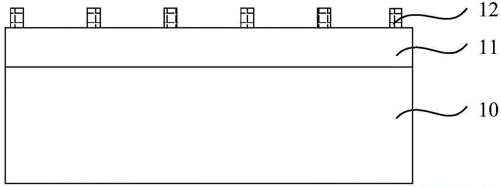
[0052] Such as Figure 7 As shown, this embodiment provides a substrate for flip-chip LED chips, including a gallium nitride substrate material 13 and a dielectric layer 12 with a patterned structure, and the dielectric layer 12 with a patterned structure is embedded in nitrogen GaN substrate material 13.

[0053] Preferably, the patterned structure is a columnar structure arranged at intervals, further, the patterned structure is a columnar structure 12a arranged periodically. Since the sides of the columnar structure are perpendicular to the surface of the substrate, the columnar structure does not have scattering or diffuse reflection. The light reflection of the substrate increases its transmission and improves the light extraction efficiency of the flip-chip LED chip, that is, increases the external quantum efficiency.

[0054] Such as Image 6 As shown, the substrate for flip-chip LED chips may also include a lattice matching layer 11 located on the surface of the gal...

Embodiment 2

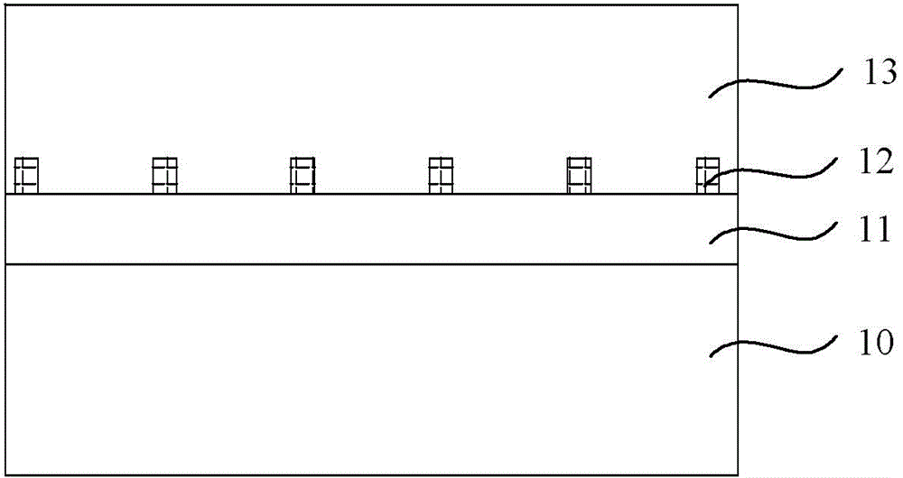
[0069] Figure 8 It is a cross-sectional view of forming a lattice matching layer and a dielectric layer on a sapphire substrate in Embodiment 2 of the present invention, Figure 9 It is a top view of the second lattice matching layer and the dielectric layer in the embodiment of the present invention.

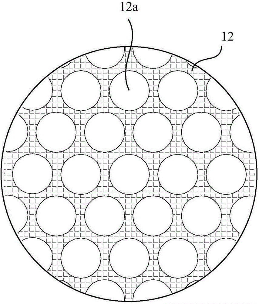
[0070] Such as Figure 8 with Figure 9 As shown, the difference between this embodiment and Embodiment 1 is that the columnar structure 12a is a columnar protrusion, and the dielectric layer 12 is composed of periodically arranged columnar protrusions, and the lattice is exposed through the gaps between the columnar protrusions. The matching layer 11, the gallium nitride substrate material 13 fills the gaps between the columnar protrusions. More specifically, the columnar structure 12a is a cylindrical protrusion. Of course, since the sapphire substrate 10 is a circular substrate, the columnar structures 12a on the edge of the sapphire substrate 10 may be incomplete cylin...

Embodiment 3

[0072] The difference between this embodiment and the first embodiment is that the columnar structure 12a is a polygonal columnar protrusion. Figure 10 It is a top view of the triple lattice matching layer and the dielectric layer according to the embodiment of the present invention. Such as Figure 10 As shown, in this embodiment, the columnar structure 12a is a hexagonal prism protrusion, the lattice matching layer 11 is exposed through the gap between the hexagonal prism protrusions, and the gallium nitride substrate material 13 is filled with Fill the spaces between the hexagonal prism-shaped protrusions.


PUM

PropertyMeasurementUnit
thicknessaaaaaaaaaa
thicknessaaaaaaaaaa

Abstract

The invention provides a substrate and an epitaxial wafer for flip LED chips and making methods thereof. The substrate comprises a gallium nitride substrate material and a dielectric layer with a graphical structure, and the dielectric layer is embedded into the gallium nitride substrate material. The substrate making method comprises the following steps: forming a lattice matching layer on a sapphire substrate; forming a dielectric layer with a graphical structure on the lattice matching layer, wherein the dielectric layer exposes part of the lattice matching layer; growing a gallium nitride substrate material on the lattice matching layer and the dielectric layer until the lattice matching layer and the dielectric layer are completely separated due to the stress of the gallium nitride substrate material; and removing at least part of the lattice matching layer. Both the gallium nitride substrate material and the dielectric layer embedded in the gallium nitride substrate material adopted by the substrate for flip LED chips provided by the invention have double functions of internal quantum efficiency increasing and external quantum efficiency increasing.

Description

technical field [0001] The invention belongs to the field of semiconductor optoelectronic chip manufacturing, in particular to a substrate for flip-chip LED chips, an epitaxial wafer and a manufacturing method thereof. Background technique [0002] Since gallium nitride (GaN)-based LEDs were commercialized in the early 1990s, after more than 20 years of development, their structures have become mature and perfect, and they have been able to meet people's current needs for lamp decoration; To replace traditional light sources and enter the lighting field, especially the high-end lighting field, the improvement of luminous brightness is the never-ending pursuit of scientific researchers in the LED industry. [0003] The root cause of the limited improvement of LED luminous brightness is the lack of natural gallium nitride substrate materials in nature. There are very few heterogeneous substrate materials that can be used for gallium nitride-based LEDs, and even fewer substrate...

Claims


Application Information

Patent Timeline
Patent Type & Authority Applications(China)
IPC IPC(8): H01L33/12H01L33/22H01L33/00
CPCH01L33/007H01L33/0093H01L33/12H01L33/22
Inventor 张昊翔丁海生李东昇赵进超黄捷陈善麟江忠永
Owner HANGZHOU SILAN AZURE
Why Eureka
Try Eureka