
Waveguide assembly

a technology of waveguides and components, applied in the direction of waveguide type devices, basic electric elements, coupling devices, etc., can solve the problems of waveguide filters, large number of separate components, and high cost of methods

Active Publication Date: 2022-06-30
HUGHES NETWORK SYST
View PDF0 Cites 0 Cited by
  • Summary
  • Abstract
  • Description
  • Claims
  • Application Information

AI Technical Summary

Benefits of technology

The present patent provides an improved waveguide assembly and a method of constructing circuit boards with waveguide filters. The assembly has a compact design, is simple and inexpensive to construct, and uses fewer components than prior designs. It has achieved high performance tolerances and uses two zero z-axis patch waveguide launches as transitions from the circuit board to the embedded RF shield with the waveguide filter. The method of constructing the assembly also provides high performance tolerances and reduces the size of the circuit board. These technical effects have led to improved performance and reduced cost of the waveguide assembly and method.

Problems solved by technology

There are several known methods of constructing circuit boards with waveguide filters, but these methods are typically expensive, require numerous separate components, and / or do not achieve high tolerances.
For example, it has been determined that strip line waveguide filters typically have high loss, require a large area of the circuit board, and are sensitive to circuit board process tolerances for high frequencies.
Waveguide filters with metal walls have a high cost and are difficult to assemble.
Waveguide filters with separate RF shields need to be large to accommodate the separate waveguide filter component, making the overall assembly bulkier and unsuitable for low cost implementations, and further increasing the cost and complexity.

Method used


Image

  • Waveguide assembly
  • Waveguide assembly
  • Waveguide assembly

Examples


Embodiment Construction

[0021]Selected embodiments will now be explained with reference to the drawings. It will be apparent to those skilled in the art from this disclosure that the following descriptions of the embodiments are provided for illustration only and not for the purpose of limiting the invention as defined by the appended claims and their equivalents.

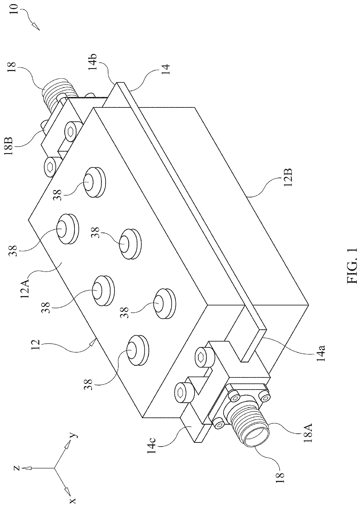
[0022]FIG. 1 illustrates an example embodiment of a waveguide assembly 10 in accordance with the present disclosure. The waveguide assembly 10 is configured to transmit an electromagnetic wave. More specifically, the waveguide assembly 10 is configured to transfer a radio frequency (“RF”) signal. It should be understood from this disclosure that the shapes, sizes and dimensions of the components of the waveguide assembly 10 will vary depending on the frequency of the RF signal to be transmitted and / or the intended application.

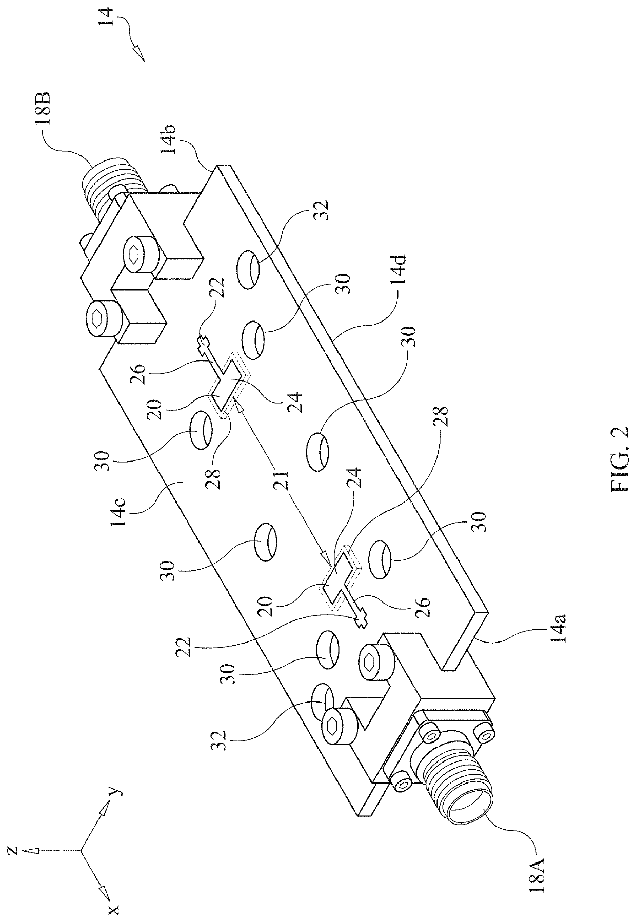
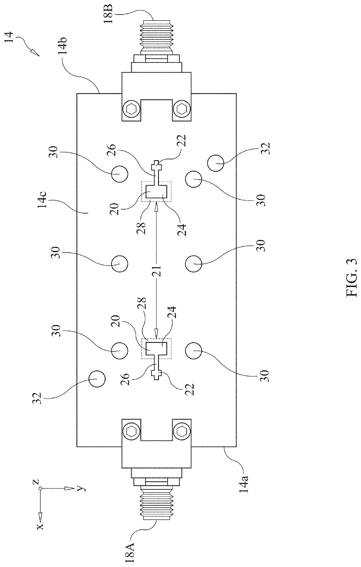
[0023]The waveguide assembly 10 includes a housing 12 and a circuit board 14. The housing 12 includes a first housing 12A a...


PUM

PropertyMeasurementUnit
resistanceaaaaaaaaaa
inner side radiusaaaaaaaaaa
electrically conductiveaaaaaaaaaa

Abstract

A waveguide assembly is disclosed herein. In an embodiment, a waveguide assembly includes a circuit board, a housing and a waveguide filter channel. The circuit board has at least one waveguide interface formed from an electrically conductive material. The housing is configured to be attached to the circuit board so as to align with the at least one waveguide interface. The waveguide filter channel is formed between the circuit board and the housing, with the circuit board and the housing each forming at least a portion of the waveguide filter channel. The waveguide filter channel is configured to at least one of (i) receive a radio frequency signal from the at least one waveguide interface or (ii) output the radio frequency signal to the at least one waveguide interface.

Description

BACKGROUNDField of the Invention[0001]The present disclosure generally relates to a waveguide assembly for use with electromagnetic waves. In particular, the present disclosure relates to a radio frequency (“RF”) waveguide assembly which integrates a waveguide filter channel into an RF shield that is attached to a circuit board.Background Information[0002]There are several known methods of constructing circuit boards with waveguide filters, but these methods are typically expensive, require numerous separate components, and / or do not achieve high tolerances. One known method is to use a strip line waveguide filter which is printed on the circuit board. Another known method is to use a waveguide filter with metal walls. Yet another known method is to mount a waveguide filter on the circuit board using a waveguide filter assembly that is separate component from the circuit board and an RF shield.SUMMARY[0003]It has been discovered that an improved waveguide assembly and method of cons...

Claims


Application Information

Patent Timeline
Patent Type & Authority Applications(United States)
IPC IPC(8): H01P1/202H01P1/20H01P1/213
CPCH01P1/202H01P1/2133H01P1/2002H01P1/207H01P5/107
Inventor CHEN, GUOLOTT, EDBROCKETT, JESSICA
Owner HUGHES NETWORK SYST
Learn More