

Power conversion device
- Summary
- Abstract
- Description
- Claims
- Application Information
AI Technical Summary
Benefits of technology
Problems solved by technology
Method used
Image

Examples
first embodiment
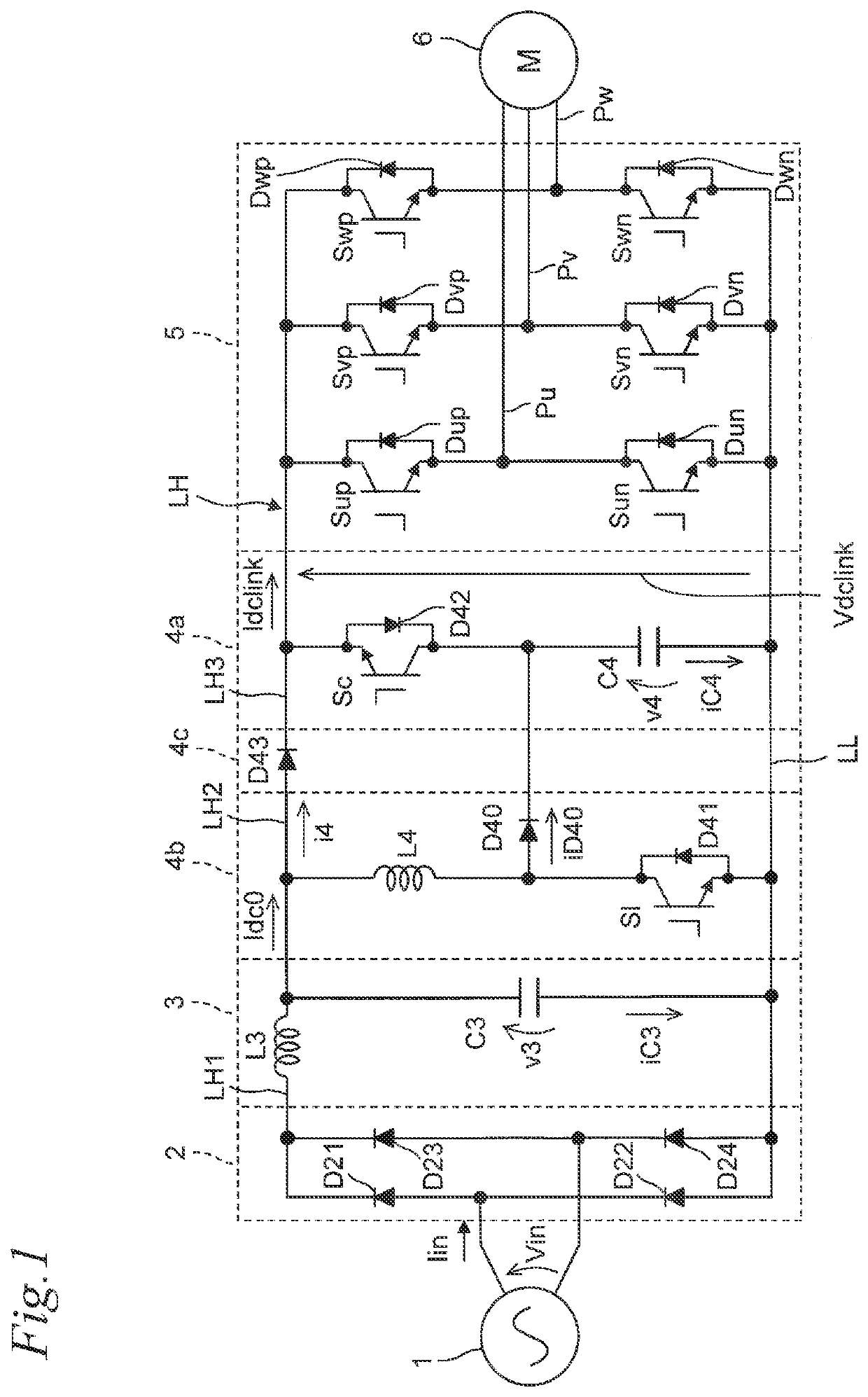
[0030]FIG. 1 is a circuit diagram of the power conversion device according to the first embodiment of the present disclosure.
[0031]As in FIG. 1, the power conversion device of the first embodiment includes a converter unit 2, a filter unit 3, a buffer circuit 4a, a charging circuit 4b, a current blocking unit 4c, an inverter unit 5, and a control device 10 (see FIG. 6). The power conversion device has a positive output end of the converter unit 2 connected to a first power source line LH, and a negative output end of the converter unit 2 connected to a second power source line LL. The first power source line LH includes a power source line part LH1 having one end connected to the positive output end of the converter unit 2, a power source line part LH2 having one end connected to the other end of the power source line part LH1 via a reactor L3, and a power source line part LH3 having one end connected to the other end of the power source line part LH2 via a diode D43.
[0032]The conve...
second embodiment
[0120]FIG. 11 is a circuit diagram of the power conversion device according to the second embodiment of the present disclosure. The power conversion device of the second embodiment has the same configuration as the power conversion device of the second embodiment except for the filter unit 3.
[0121]In the power conversion device of the second embodiment, as in FIG. 11, the converter unit 2 is connected to the single-phase alternating current power source 1 via the filter unit 3. The filter unit 3 includes the reactor L3 and the capacitor C3. The reactor L3 is provided between one output end of the single-phase alternating current power source 1 and one input end of the converter unit 2. The capacitor C3 is provided between two output ends of the single-phase alternating current power source 1. The filter unit 3 removes a high-frequency component of the current.
[0122]The power conversion device of the second embodiment performs the first conversion operation and the second conversion ...
third embodiment
[0130]FIG. 13 is a circuit diagram of the power conversion device according to the third embodiment of the present disclosure. The power conversion device of the third embodiment has the same configuration as the power conversion device of the second embodiment except for a rectifying unit 7 and the circuit configuration.
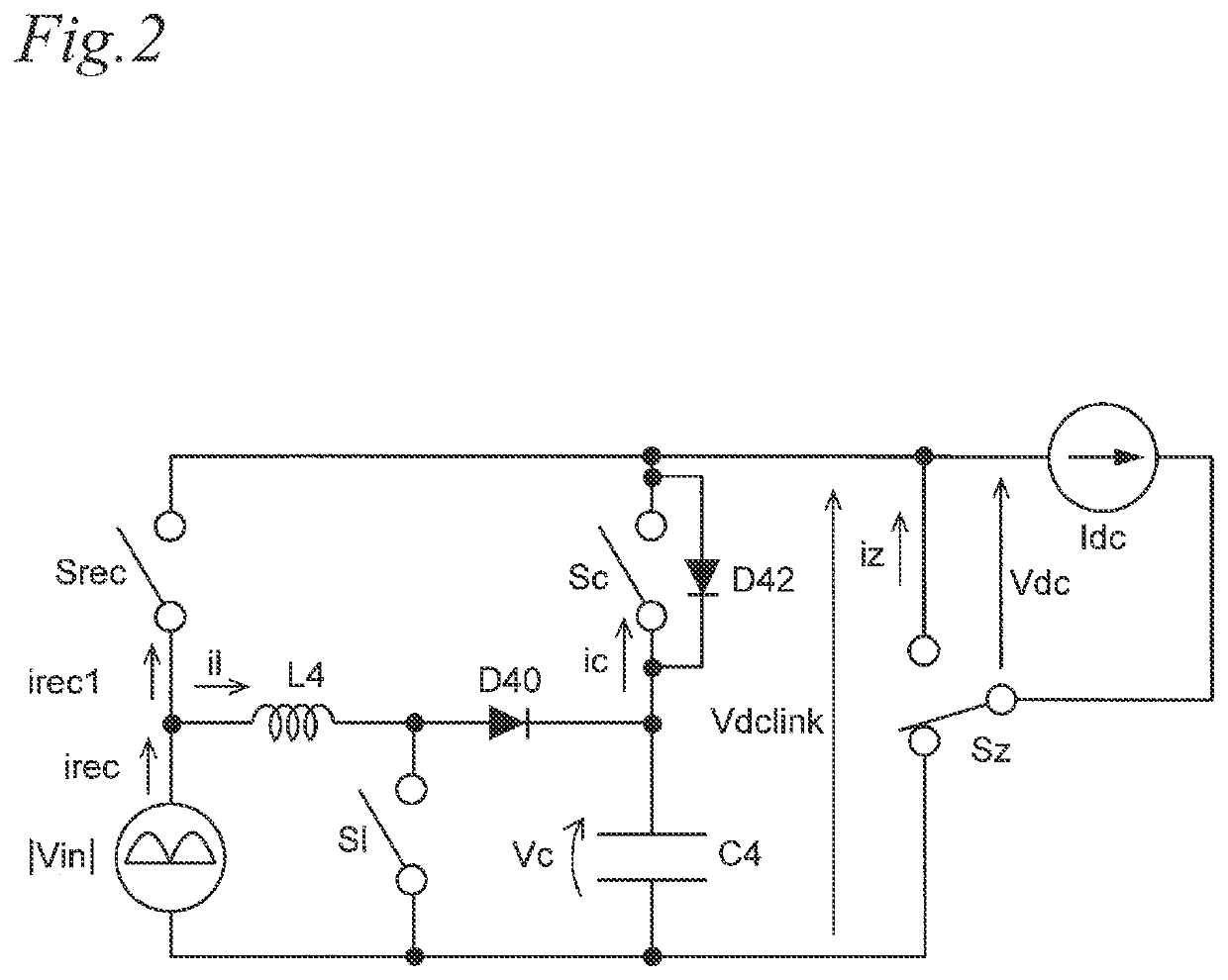
[0131]In the power conversion device of the third embodiment, the filter unit 3 is connected to the first power source line LH on the input side of the buffer circuit 4a via the rectifying unit 7. The rectifying unit 7 outputs a rectified voltage by single-phase full-wave rectification on the single-phase alternating current voltage Vin input from the single-phase alternating current power source 1.
[0132]One end of the charging circuit 4b on the reactor L4 side is connected to the positive output end of the converter unit 2 via a third power source line LH4. The other end of the charging circuit 4b is connected to the negative output end of the converter unit 2 via ...
PUM
 Abstract
Description
Claims
Application Information