Unlock instant, AI-driven research and patent intelligence for your innovation.
Active matrix substrate
Pending Publication Date: 2022-08-11
SHARP KK
View PDF0 Cites 0 Cited by
Summary
Abstract
Description
Claims
Application Information
AI Technical Summary
This helps you quickly interpret patents by identifying the three key elements:
Problems solved by technology
Method used
Benefits of technology
Benefits of technology
The patent embodiment describes a display screen that has multiple TFTs (the active matrix substrate) on it. These TFTs have a unique structure called a top-gate, which makes them efficient and effective at displaying images. The TFTs have either a light-shielding or transparent lower electrode, depending on their specific needs and functions in the display. The technical effect of this patent text is to provide a more efficient and effective display screen for better user experience.
Problems solved by technology
A possible reason behind this is that the duty ratio of the driving signal applied to the gate differs between the pixel TFTs and the SSD circuit TFTs, and this leads to deterioration phenomena (the threshold voltage shift direction, the shift amount, etc.) different from one another.
Thus, when multiple oxide semiconductor TFTs having different driving signal duty ratios are formed on the same substrate, it is difficult to sufficiently suppress deterioration of characteristics and extend the lifetime of all TFTs, and there is a possibility that the reliability of the active matrix substrate would be degraded.
Method used
Image
Click on the blue label to locate the original text in one second.
Reading with bidirectional positioning of images and text.
Examples
first embodiment
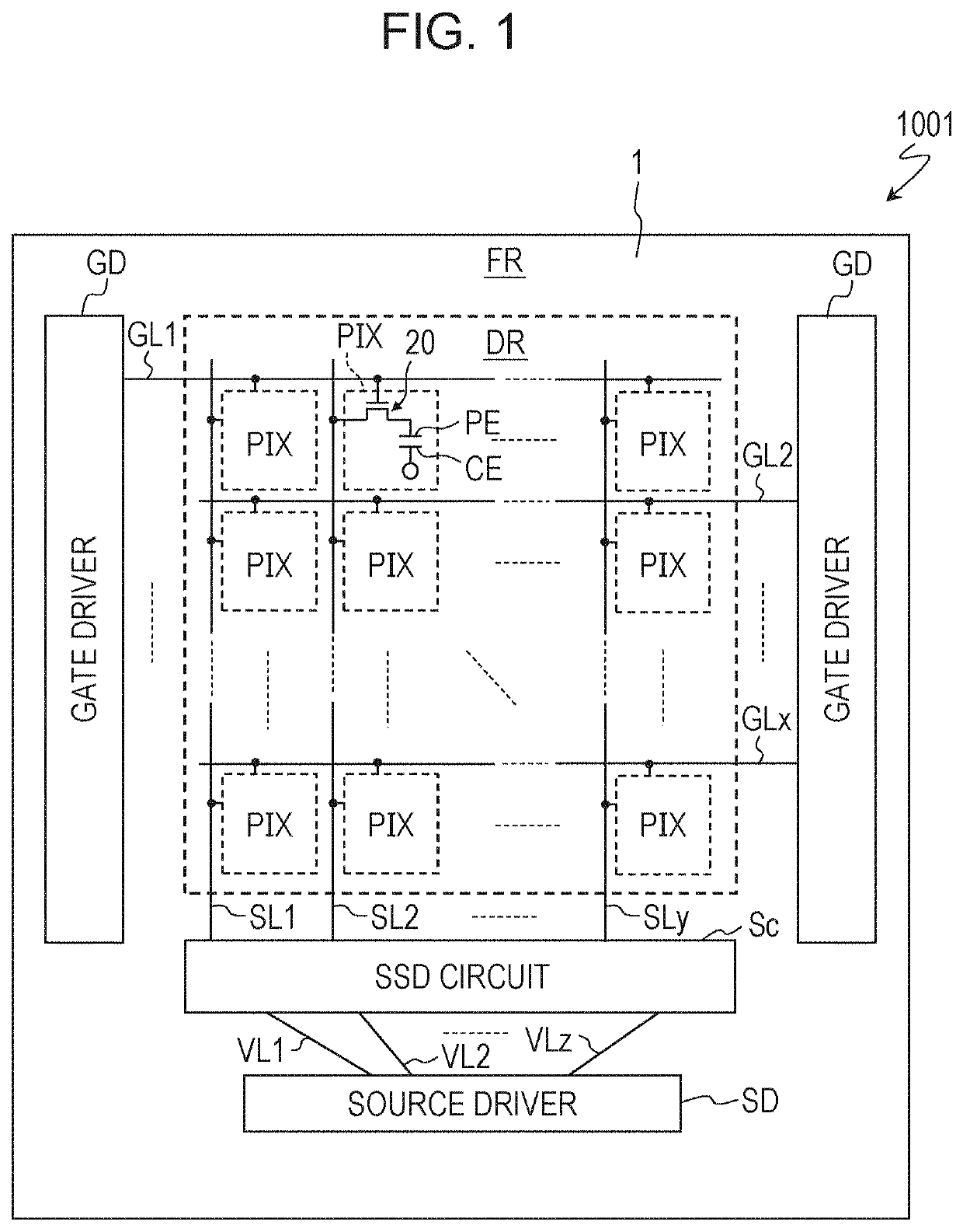
[0054]Hereinafter, an active matrix substrate of a first embodiment is described with reference to the drawings.
[0055]FIG. 1 is a schematic diagram illustrating one example of a planar structure of an active matrix substrate 1001. The active matrix substrate 1001 has a display region DR that contributes to displaying and a peripheral region (frame region) FR positioned outside the display region DR. The display region DR includes multiple pixel regions PIX arranged into a matrix. A pixel region PIX (may be simply referred to as a “pixel”) is a region that corresponds to a pixel of a display device. The non-display region FR is positioned in the periphery of the display region DR and does not contribute to displaying.
[0056]The active matrix substrate 1001 is equipped with, in a display region DR, a substrate 1, multiple pixel TFTs 20 supported on the substrate 1, multiple pixel electrodes PE, multiple gate bus lines GL1 to GLx (x is an integer of 2 or more, hereinafter, may be collec...
modification examples
[0108]Hereinafter, modification examples of the active matrix substrate of this embodiment are described with reference to the drawings. In the drawings hereinafter, constitutional elements similar to those illustrated in FIGS. 2A to 3B are denoted by the same reference signs.
[0109]The descriptions of similar features may be omitted as appropriate.
modification example 1
[0110]FIG. 4A is a plan view illustrating a first TFT 101 and a second TFT 201 of an active matrix substrate 1001 according to modification example 1. FIG. 4B is a cross-sectional view taken along line IVB-IVB in FIG. 4A. Furthermore, FIG. 5 is a cross-sectional view taken along line V-V in FIG. 4A.
[0111]The first TFT 101 of modification example 1 differs from the first TFT 100 illustrated in FIGS. 2A and 2B in that, in the lower electrode 3A, the first metal film m1 is disposed on the first transparent conductive film t1. In this modification example also, as with the first TFT 100, the first metal film m1 that serves as a light-shielding portion 31m is arranged to overlap the entire channel region 61c when viewed in the normal direction of the substrate 1. Other features are the same as those of the first TFT 100.
[0112]Meanwhile, the second TFT 201 has the same structure as the second TFT 200 illustrated in FIGS. 2A and 2B.
[0113]The active matrix substrate 1001 of this modificatio...
PUM
Abstract
An active matrix substrate includes first and second TFTs. The first TFT includes a first lower electrode, a first insulating layer, a first oxidesemiconductor layer, and a first gate electrode. The first oxidesemiconductor layer includes a first channel region overlapping the first gate electrode when viewed in a normal direction of the substrate. The first lower electrode has a first light-shielding portion overlapping the entire first channel region and including a first metal film. The second TFT includes a second lower electrode, the first insulating layer, a second oxidesemiconductor layer, and a second gate electrode. The second oxide semiconductor layer includes a second channel region overlapping the second gate electrode when viewed in the normal direction. The second lower electrode has a light-transmitting portion overlapping the second channel region and including a first transparent conductive film but not a light-shielding metal film.
Description
BACKGROUND1. Field[0001]The present disclosure relates to an active matrix substrate.2. Description of the Related Art[0002]An active matrix substrate used in a display device includes a display region that includes multiple pixel regions and a non-display region (also referred to as a “frame region” or a “peripheral region”) other than the display region. A pixel region is a region that corresponds to a pixel of a display device. Each of the pixel regions is equipped with a thin film transistor (hereinafter also referred to as a “TFT”) that serves as a switching element.[0003]In recent years, use of oxide semiconductors instead of amorphous silicon and polycrystalline silicon as the material for active layers of TFTs has been proposed. Such TFTs are referred to as “oxide semiconductor TFTs”. Oxide semiconductors have higher mobility than amorphous silicon. Thus, oxide semiconductor TFTs can operate with higher speed than amorphous silicon TFTs. Moreover, since oxide semiconductor f...
Claims
Application Information
Patent Timeline
Application Date:The date an application was filed.
Publication Date:The date a patent or application was officially published.
First Publication Date:The earliest publication date of a patent with the same application number.
Issue Date:Publication date of the patent grant document.
PCT Entry Date:The Entry date of PCT National Phase.
Estimated Expiry Date:The statutory expiry date of a patent right according to the Patent Law, and it is the longest term of protection that the patent right can achieve without the termination of the patent right due to other reasons(Term extension factor has been taken into account ).
Invalid Date:Actual expiry date is based on effective date or publication date of legal transaction data of invalid patent.

