Semiconductor device having a structure for detecting a boosted potential

a technology of boosted potential and booster, which is applied in the direction of semiconductor devices, semiconductor/solid-state device details, electrical apparatus, etc., can solve the problems that the booster cannot raise the input voltage to a desired voltage, and the desired voltage raising operation cannot be achieved

Inactive Publication Date: 2000-01-04
RENESAS ELECTRONICS CORP
View PDF5 Cites 12 Cited by
  • Summary
  • Abstract
  • Description
  • Claims
  • Application Information

AI Technical Summary

Problems solved by technology

Flow of a large current through the raised potential measuring circuit indicates current leakage in the booster and, if current leaks from the booster, the booster cannot raise the input voltage to a desired voltage.
Such penetration 43 forms an unnecessary high resistance portion or an unnecessary current path, so that the desired voltage raising operation cannot be achieved.

Method used


Image

  • Semiconductor device having a structure for detecting a boosted potential
  • Semiconductor device having a structure for detecting a boosted potential
  • Semiconductor device having a structure for detecting a boosted potential

Examples


first embodiment

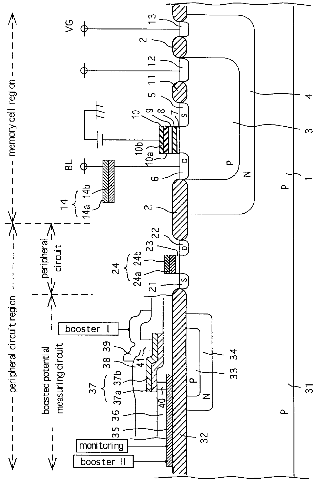
A wiring structure for a raised potential measuring circuit according to a first embodiment of the present invention and a semiconductor device having the inventive raised potential measuring circuit will now be described with reference to the accompanying drawings. By way of example, a raised potential measuring circuit included in a DINOR type flash memory will be explained.

A memory cell region and a peripheral circuit region are shown in a right-hand section and a left-hand section, respectively, of FIG. 1.

First, the memory cell region in the right-hand section will be described. FIG. 1 depicts a p-type semiconductor substrate 1 of silicon or the like, an isolating oxide film 2 formed on a surface of the semiconductor substrate 1, a p-type well 3 formed in a predetermined region of the surface of the p-type semiconductor substrate 1, and an n-type well 4 formed in the p-type semiconductor substrate 1 so as to cover the bottom surface and the side surface of the p-type well 3.

FIG....


PUM


Abstract

A p-type well and an n-type well surrounding the p-type well are formed in a p-type semiconductor substrate under a field insulating film. A polysilicon resistance film is formed on the field insulating film simultaneously with a floating gate formed in a memory cell region. A polycide conductive film is formed on a interlayer insulating film simultaneously with an auxiliary bit line formed in the memory cell region, and the polycide conductive film is connected to the resistance film by a contact formed in a via hole. A wiring line formed on an interlayer insulating film is connected to the polycide conductive film by a contact formed in a via hole penetrating the interlayer insulating film. The two via holes are formed at positions corresponding to regions in the p-type well. A negative voltage is applied to the wiring line, and the potential of a predetermined point on the resistance film is measured.

Description

1. Field of the InventionThe present invention relates to a semiconductor device with an internal booster and a structure for detecting a boosted potential, and more specifically, to improvements in a connecting structure for connecting a negative potential to a resistor film in a raised potential measuring circuit in a semiconductor device.2. Background ArtIn a semiconductor memory device, such as an EEPROM, requiring a high voltage for writing and erasing data from memory cells, a positive or negative supply voltage must be raised and the raised voltage must be measured to see whether or not the supply voltage has been raised to a desired voltage.FIG. 4 is a block diagram showing a raised potential measuring circuit. A voltage generated by a booster I or a booster II is connected to a resistance film 35, and potential at a predetermined point in the resistance film 35 is monitored to see whether or not the output voltage of booster I or booster II is appropriate.A 16 Mb DINOR type...

Claims


Application Information

Patent Timeline
Patent Type & Authority Patents(United States)
IPC IPC(8): H01L21/70H01L21/8247H01L27/105H01L27/10H01L27/115H01L29/788H01L29/792
CPCH01L27/105H01L27/11526H01L27/11541H10B41/40H10B41/47H01L27/10
Inventor YUZURIHA, KOJIROOOI, MAKOTOKOBAYASHI, SHINICHI
Owner RENESAS ELECTRONICS CORP
Why Eureka
Try Eureka