Clock signal generator for generating a plurality of clock signals with different phases, and clock phase controller using the same

Inactive Publication Date: 2000-02-01
RENESAS ELECTRONICS CORP
View PDF10 Cites 59 Cited by
  • Summary
  • Abstract
  • Description
  • Claims
  • Application Information

AI Technical Summary

Problems solved by technology

The conventional pixel pulse generator 60, however, cannot be implemented as an integrated circuit through a CMOS process because it includes the triangular wave generator 66 consisting of an analog circuit.
However, the following problems arises from applying such a phase conversion

Method used


Image

  • Clock signal generator for generating a plurality of clock signals with different phases, and clock phase controller using the same
  • Clock signal generator for generating a plurality of clock signals with different phases, and clock phase controller using the same
  • Clock signal generator for generating a plurality of clock signals with different phases, and clock phase controller using the same

Examples


embodiment 1

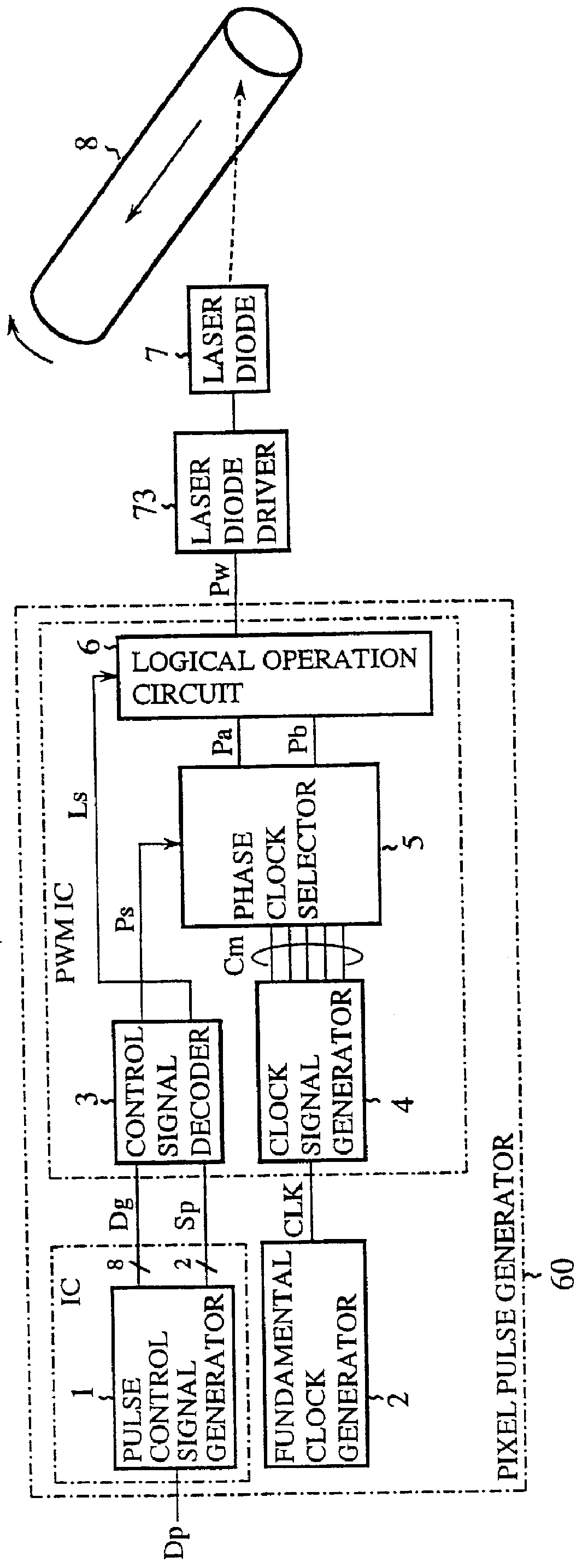
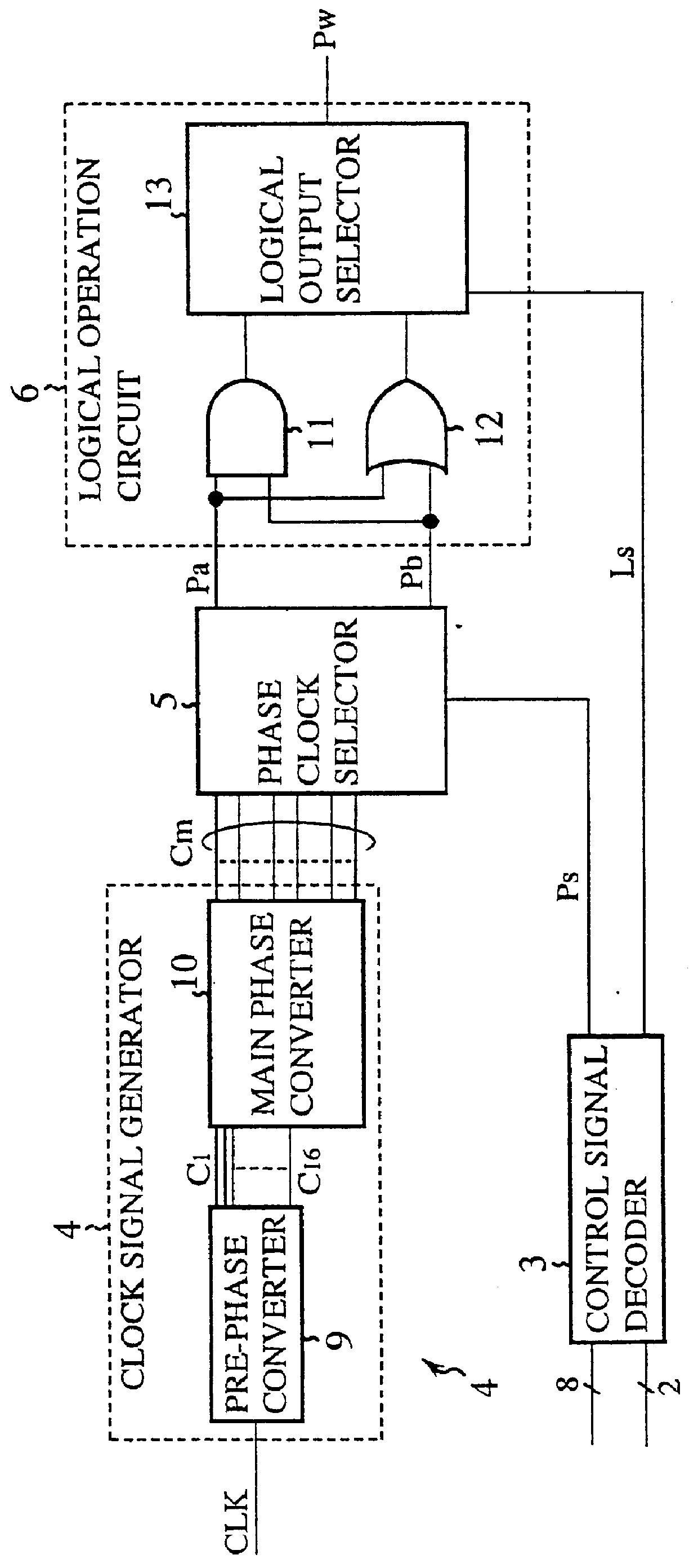
FIG. 1 is a block diagram showing a configuration of an image output portion of a laser printer, to which an embodiment 1 is applied of the pulse-width modulation signal generator in accordance with the present invention. In FIG. 1, the reference numeral 60 designates a pixel pulse generator that receives in series pixel data Dp, elements of an image, and produces a pulse-width modulation signal Pw in response to the pixel data Dp; 73 designates a laser diode (LD) driver that receives the pulse-width modulation signal Pw and outputs a drive signal; 7 designates a laser diode that receives the drive signal and emits a light beam in accordance with the pulse width of the pulse-width modulation signal Pw; and 8 designates a photoconductive drum on which the light beam emitted from the laser diode 7 is thrown so that a latent electrostatic image is formed as the charge distribution corresponding to the scanning of the emitted light beam.

The reference numeral 1 designates a pulse control...

embodiment 2

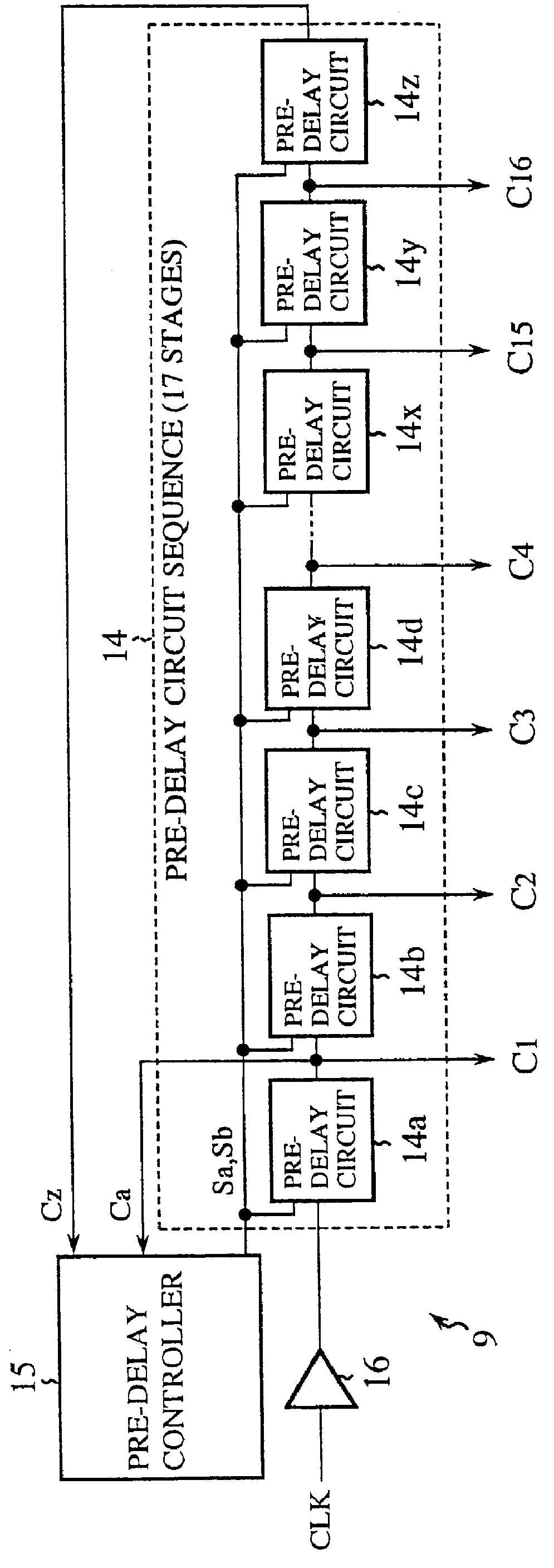
FIG. 9 is a block diagram showing the pre-phase converter 9 of an embodiment 2 in accordance with the present invention. In FIG. 9, the reference numeral 29 designates a dividing ratio decoder for decoding a dividing ratio data Dd that is set for the pulse-width control IC. The reference numeral 30 designates a dividing ratio selector which, receiving an output signal Ds of the dividing ratio decoder 29 and the pre-delay clock signals C2-C16 and Cz0 output from a set of 16 pre-delay circuits from the second one 14b to the final one 14z, selects one of the 16 pre-delay clock signals in response to the output signal Ds of the dividing ratio decoder 29, and outputs the selected one as a select delay clock signal Cz. The reference numeral 31 designates a delay circuit with a delay time identical to the transfer delay of the clock signal through the dividing ratio selector 30. Since the remaining configuration is the same as that of the embodiment 1, description thereof is omitted here b...

embodiment 3

FIGS. 10A and 10B are block diagrams showing a configuration of the pre-phase converter 9 of an embodiment 3 in accordance with the present invention. In FIG. 10A, the reference numeral 32 designates a delay amount decoder for decoding delay setting data Dst which is set in the pulse-width control IC. The output Sd of the delay amount decoder 32 is input to the entire pre-delay circuits 14a-14z. FIG. 10B is a block diagram showing a configuration of each of the pre-delay circuits 14a-14z. In FIG. 10B, reference numerals 17 each designate a buffer, and 34 designates a unit delay time selector 34 for selecting one of the outputs of the five buffers 17 in response to the selection signal Sd fed from the delay amount decoder 32. Since the remaining configuration is the same as that of the embodiment 1, description thereof is omitted here by designating like portions by the same reference numerals.

Next, the operation of the pre-phase converter 9 of the present embodiment 3 will be descri...


PUM


Abstract

A clock signal generator having a pre-phase converter for generating in response to an input clock signal a plurality of pre-delay clock signals with different phases; and main phase converters each of which receives one of the pre-delay clock signals, and generates a plurality of main delay clock signals with their phases different from each other, thereby generating multiple main delay clock signals with their phases different from each other.

Description

1. Field of the InventionThe present invention relates to a clock signal generator for generating a plurality of clock signals with different phases and a clock phase controller using the same, and particularly to a clock signal generator and clock phase controller using the same preferably used for controlling a light emitting device such as a laser diode in an electrophotographic image forming apparatus like a laser printer.2. Description of Related ArtFIG. 15 is a block diagram showing a configuration of an image output portion of a conventional laser printer. In FIG. 15, the reference numeral 60 designates a pixel pulse generator that receives pixel data Dp in series which are elements of an image and produces a pulse-width modulation signal Pw in response to each of the pixel data Dp; 73 designates a laser diode driver that receives the pulse-width modulation signal Pw and outputs a drive signal; 61 designates a laser diode for emitting a light beam in response to the drive sig...

Claims


Application Information

Patent Timeline
IPC IPC(8): H03L7/081H03L7/07H03K5/135H03L7/08H03K5/13H03K5/15H03L7/093
CPCH03K5/13H03K5/135H03L7/07H03L7/0805H03L7/0812H03K5/133
Inventor KAN, YASUHIROTANIGUTI, MASAHARU
Owner RENESAS ELECTRONICS CORP
Why Eureka
Try Eureka