

Dielectric waveguide
a technology of dielectric waveguides and waveguides, applied in waveguides, slot antennas, antennas, etc., can solve the problem of the same difficulty
- Summary
- Abstract
- Description
- Claims
- Application Information
AI Technical Summary
Problems solved by technology
Method used
Image

Examples
first embodiment
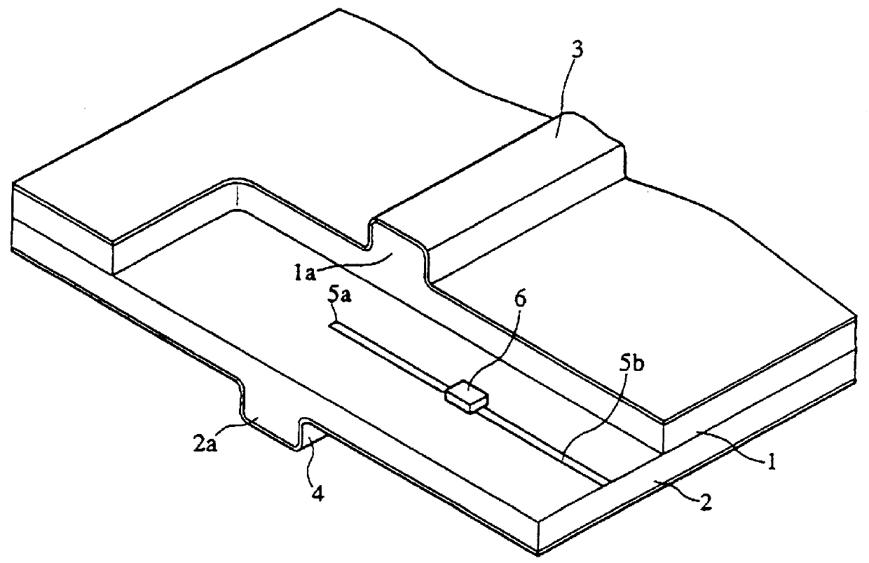
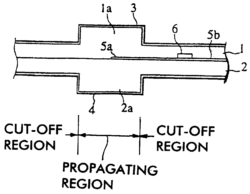
FIGS. 1A and 1B show the structure of a dielectric waveguide according to a first embodiment of the present invention. Dielectric substrates 1 and 2 are laminated. The dielectric substrates 1 and 2 have projections 1a and 2a respectively. The dielectric substrates are laminated so that the projections 1a and 2a are aligned. Electrodes 3 and 4 are provided on substantially the whole outer surface of each dielectric substrate.
The dielectric provided within and between the projections 1a and 2a, and between the pair of opposing electrodes 3 and 4, forms a propagating region. Dielectric between the pair of electrodes 3 and 4, other than in the propagating region, forms a cut-off region. Line conductors 5a and 5b may be provided on the dielectric substrate 1. Line conductor 5a may be extended into the propagating region. In the propagating region, the line conductor 5a, the electrodes 3 and 4, and the dielectric within the projections form a Triplate line.
An electronic component 6, such ...
second embodiment
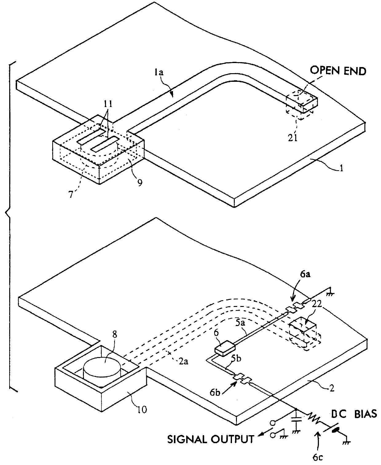
The structure of a dielectric waveguide according to a second embodiment of the present invention is explained with reference to FIGS. 2, 3, 4A and 4B. A pair of dielectric substrates 1 and 2 are laminated as shown in FIG. 3 wherein the dielectric substrates are separately shown for the sake of convenience.
FIG. 3 shows the dielectric waveguide according to a second embodiment of the present invention. FIG. 4A is a sectional view taken along line A--A in FIG. 3. FIG. 4B is a sectional view taken along line B--B in FIG. 3.
Similar to the dielectric waveguide according to the first embodiment, the dielectric within and between the projections 1a and 2A (not shown), and between electrodes 3 and 4, forms a propagating region. The electrodes 3, 4 may be electrode layers formed on substantially the entire exterior surfaces of the dielectric substrates 1 and 2.
Also shown are a pair of extension parts 9 and 10 which extend respectively from the dielectric plates 1 and 2, at corresponding ends...
third embodiment
Next, a dielectric waveguide according to a third embodiment of the present invention is explained, referring to FIGS. 5-7B. Hollows 18 and 19 are provided between the ends of a propagating region, halfway along its length in this example. An alignment of hollows 18 and 19 forms a cavity in the middle of the propagating region. A dielectric filter 12 is inserted into the cavity.
The dielectric filter 12 comprises electrodes 13 and 14 arranged respectively on the upper and lower surfaces of a dielectric substrate 17. Openings 15a and 15b are formed in the electrodes 13. Openings 16a and 16b of the same shape are provided in the electrode 17. The openings 15a and 16a, and the openings 15b and 16b, oppose respectively.
The cross section of the above-mentioned dielectric filter is shown in FIG. 6. The area between the openings 15a and 16a, and the area between the openings 15b and 16b, form respective TE010 mode dielectric resonators. As shown in FIG. 7A, the dielectric filter 12 is provi...
PUM
 Abstract
Description
Claims
Application Information