
Method for fabricating a photomask

Inactive Publication Date: 2000-06-06
UNITED MICROELECTRONICS CORP
View PDF2 Cites 11 Cited by
  • Summary
  • Abstract
  • Description
  • Claims
  • Application Information

AI Technical Summary

Problems solved by technology

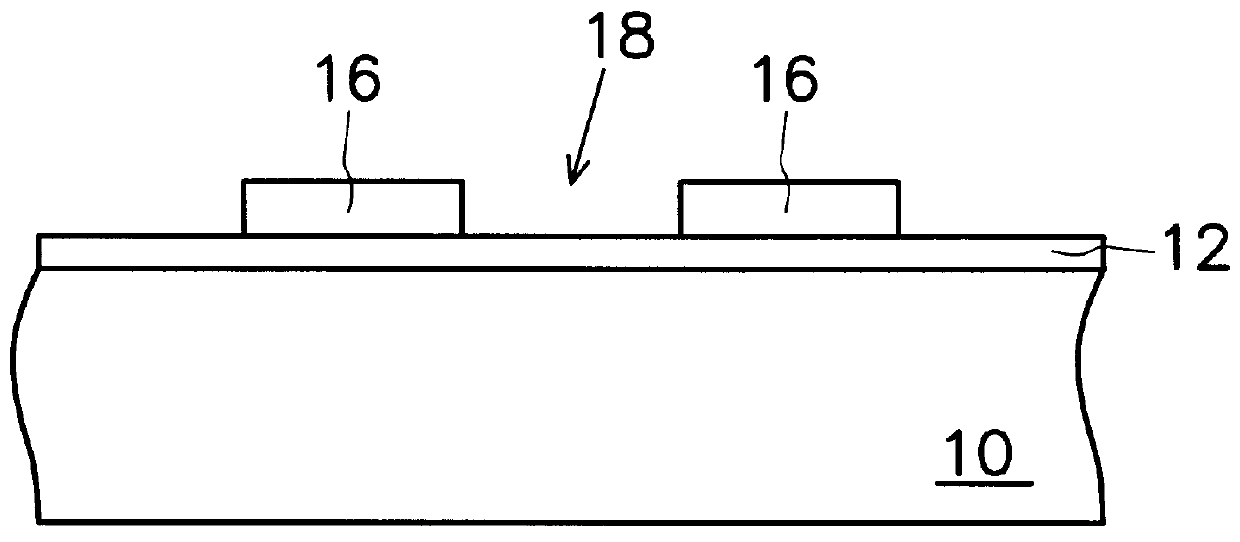
However, since the transparent region 18 and the opaque region 16 are formed by photolithography and etching, their spatial resolution is limited by equipment capability of photolithography.
This is a problem for semiconductor fabrication in the next generation, which has greater integration.

Method used


Image

  • Method for fabricating a photomask
  • Method for fabricating a photomask
  • Method for fabricating a photomask

Examples


Embodiment Construction

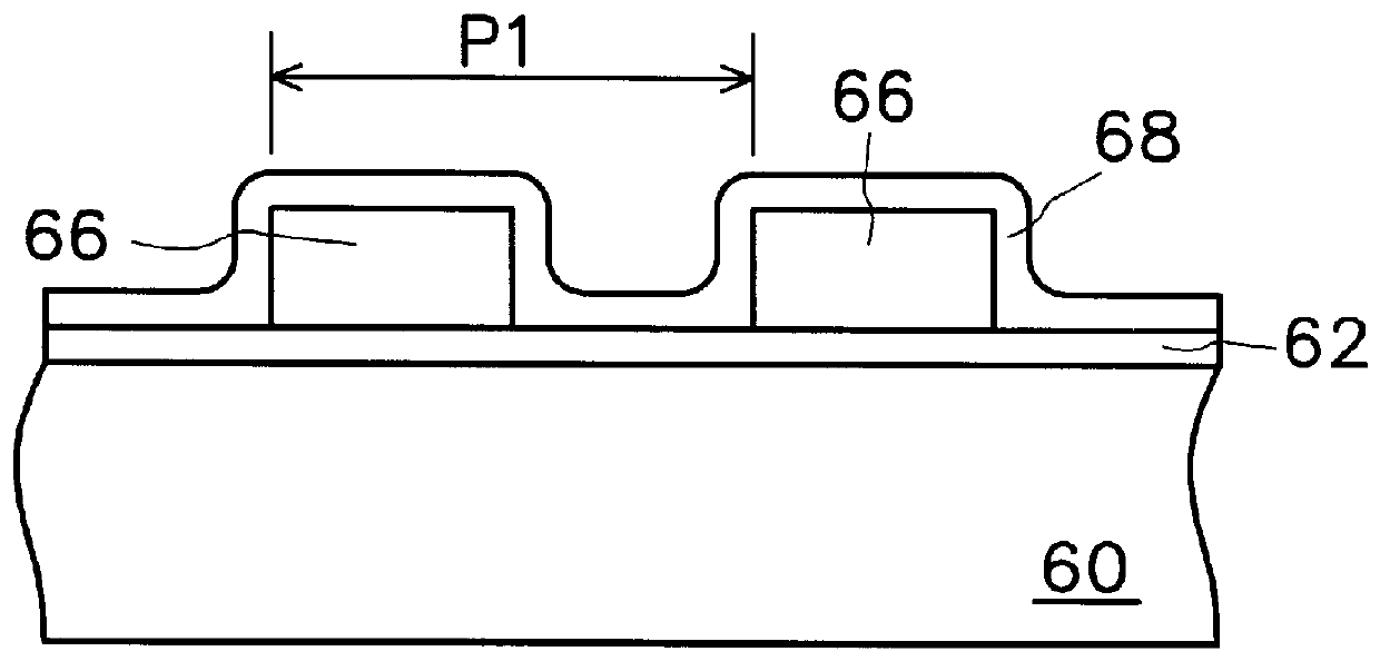
FIGS. 2A-2F are cross-sectional views of a photomask, schematically illustrating a fabrication process of the photomask, according to a preferred embodiment of the invention. In FIG. 2A, a transparent substrate 60 including, for example, quartz or silicon glass is provided. The choice of material depends on the wavelength of a light source. An anti-reflection layer 62 is formed over the transparent substrate 60. The anti-reflection layer 62 includes, for example, CrO.sub.2 and is used to prevent a light reflection during a subsequent metallization process. A transparent layer 64 is formed over the anti-reflection layer 62. The transparent layer 64 includes, for example, silicon oxide and is formed by, for example, chemical vapor deposition (CVD).

In FIG. 2B, the transparent layer 64 is patterned to form a transparent bar layer 66. A portion of the anti-reflection layer 62 is exposed. An opaque layer 68 is formed over the transparent substrate 60 so that the anti-reflection layer 62 a...


PUM


Abstract

A method for fabricating a photomask includes forming an anti-reflection layer on a transparent substrate. A transparent layer is formed on the anti-reflection layer. Patterning the transparent layer forms a transparent bar layer so that a portion of the ant-reflection layer is exposed. An opaque layer is formed over the substrate. A polishing process is performed to polish the opaque layer and the transparent bar layer so that a top portion of the transparent bar layer is polished and exposed. An etching back process is performed to remove a portion of the opaque layer so that the anti-reflection layer is exposed and the remains of the opaque layer forms a spacer with uniform thickness on each side of the transparent bar layer. The transparent bar layer is removed by etching so as to form the photomask.

Description

1. Field of the InventionThis invention relates to semiconductor fabrication, and more particularly to a method for fabricating a photomask, which has a pattern including a narrow line width and a small pitch between lines.2. Description of Related ArtIn a photolithography process, photomask is the main tool to transfer a circuit pattern onto a wafer so that the photomask plays an essential role in semiconductor fabrication. The main part of the photomask is a transparent substrate and is planar. A circuit pattern is formed by an opaque layer, which includes a desired pattern to cover a portion of the transparent substrate. When the photomask is exposed to a light source, a circuit pattern is projected onto the wafer. As the integration of a device increases, the photomask needs a narrower line width to satisfy the reduced device dimension.FIG. 1A and FIG. 1B are cross-sectional views of a photomask, schematically illustrating a conventional fabrication process of the photomask. In ...

Claims


Application Information

Patent Timeline
IPC IPC(8): G03F1/14G03F7/00G03F1/00G03F1/46
CPCB82Y10/00G03F1/46G03F1/14G03F1/50
Inventor LIN, BENJAMIN SZU-MIN
Owner UNITED MICROELECTRONICS CORP
Learn More