Ferroelectric capacitor and integrated circuit device comprising same

a ferroelectric capacitor and capacitor technology, applied in the direction of capacitor details, electrical apparatus, capacitors, etc., can solve the problems of ferroelectric material deformation, direct reaction of silicon dioxide, and deformation of ferroelectric material electrical properties,

Inactive Publication Date: 2000-06-06
HANGER SOLUTIONS LLC
View PDF54 Cites 63 Cited by
  • Summary
  • Abstract
  • Description
  • Claims
  • Application Information

AI Technical Summary

Problems solved by technology

Silicon dioxide appears to be a very good choice as the intermetal layer material except that in combination with the ferroelectric material, it creates problems while it is being deposited or during subsequent processing steps.
A primary problem is that silicon dioxide reacts directly with the exposed parts of PbZrTiO.sub.3 or SrBi.sub.2 Ta.sub.2 O.sub.9 while the silicon dioxide is being deposited or during the subsequent processing steps.
This reaction degrades the electrical properties of the ferroelect

Method used


Image

  • Ferroelectric capacitor and integrated circuit device comprising same
  • Ferroelectric capacitor and integrated circuit device comprising same
  • Ferroelectric capacitor and integrated circuit device comprising same

Examples


Embodiment Construction

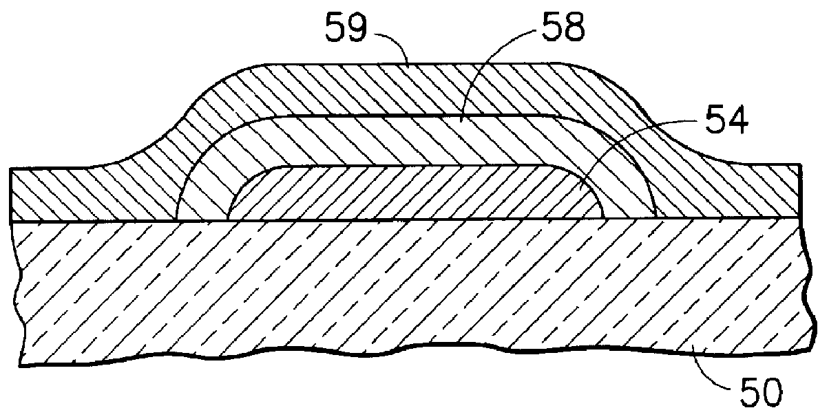
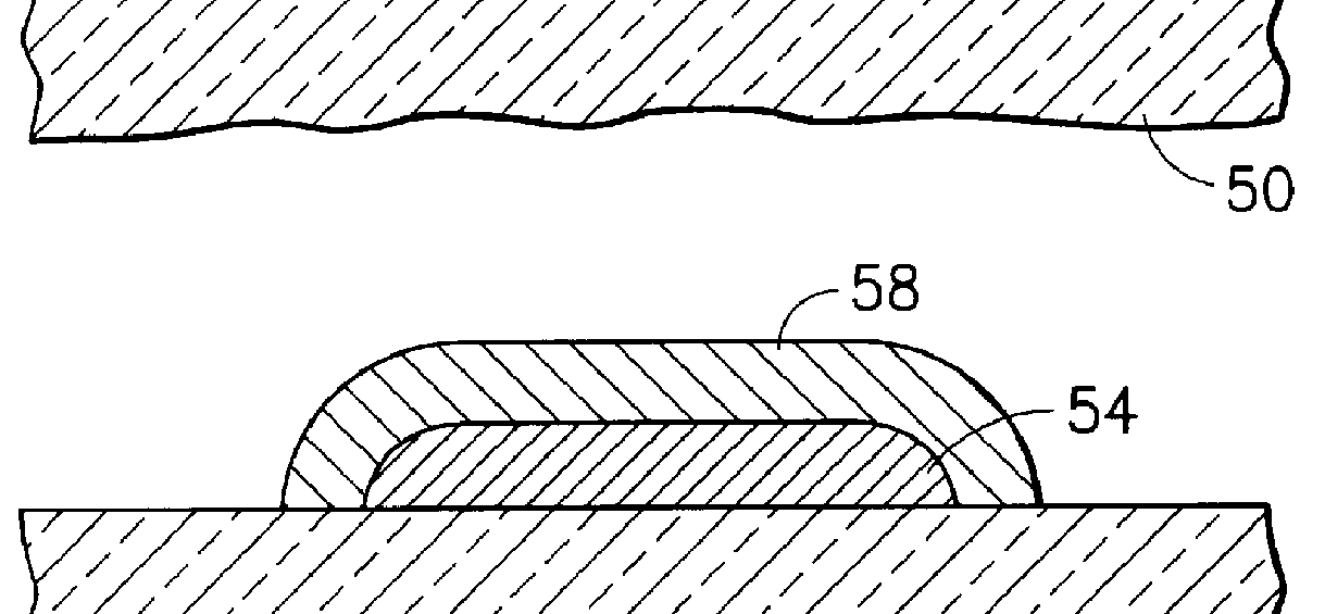
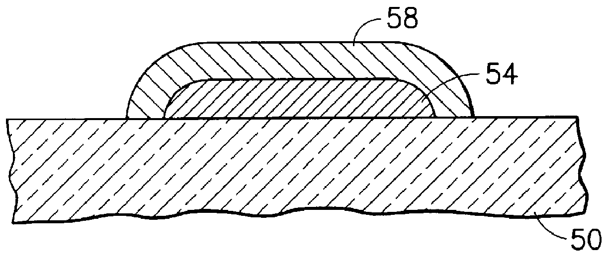
Referring now to FIG. 1, there is shown a semiconductor substrate 50 that has a conductive layer of material 52 deposited thereupon. This layer of conductive material 52 may be any compatible conductor, such as a metal. Typical metallic conductors include aluminum (Al), copper (Cu) and tungsten (W). The metallic conductor may be suitably deposited by a chemical vapor deposition (CVD) process, using well-known apparatus and processing parameters. After the layer of conductive material 52 is deposited on the substrate 50, then the conductive material is formed into a desired shape of a capacitor plate by conventional techniques well-known in the art.

FIG. 2 shows the result of the steps of processing the device, as shown in FIG. 1, to form the first plate 54 of a capacitor that may be used as the storage capacitor in an integrated circuit memory device. In the process steps, a photoresist is deposited over the layer of conductive material 52 of FIG. 1. The photoresist is patterned, and...


PUM


Abstract

An integrated circuit capacitor in which a first conductive plate, a layer of ferroelectric material, and a second conductive plate are deposited and formed in sequence. Thereafter a diffusion barrier material and an insulative material are deposited either as a layered dielectric stack with alternating layers of the diffusion barrier material and the insulative material with tensile and compressive stresses in the alternating layers offsetting one another, or as a graded diffusion barrier material varying from a binary oxide of Ta, Nb, or Zr at the surface of the ferroelectric material to SiO2 at a distance above the surface of the ferroelectric material.

Description

1. Field of the InventionThis invention relates to devices methods for fabricating integrated circuits and more particularly to a method for fabricating a ferroelectric capacitor in an integrated circuit (IC) device, as well as the ferroelectric capacitor structure and the IC device comprising same.2. Description of the Related ArtIntegrated circuit chips include a substrate of semiconductive material with component structures of electronic circuits, e.g., transistors and resistors, fabricated within the substrate structure. Additional electrical devices and precursor and / or component structures of the electronic circuits are fabricated over the top of the substrate. These additional devices and structures of circuits include conductive leads, capacitors, and parts of transistors. The devices fabricated above the substrate typically require many layers, of a variety of materials, e.g., conductors, semiconductors, insulators, and barriers.Conductive layers in integrated circuit devic...

Claims


Application Information

Patent Timeline
IPC IPC(8): H01L21/02H01L21/316
CPCH01L21/31691H01L28/60H01L28/55H01L21/02197
Inventor KIRLIN, PETER S.
Owner HANGER SOLUTIONS LLC
Why Eureka
Try Eureka