Crystal growth observing apparatus using a scanning tunneling microscope

a scanning tunneling microscope and crystal growth technology, applied in the direction of crystal growth process, polycrystalline material growth, instruments, etc., can solve the problems of inability to estimate individual real spaces at the atomic level, and the observation of stm in the mbe device is, in fact, very difficul

Inactive Publication Date: 2000-06-13
NATIONAL RESEARCH INSTITUTE FOR METALS SCIENCE AND TECHNOLOGY AGENCY
View PDF4 Cites 2 Cited by
  • Summary
  • Abstract
  • Description
  • Claims
  • Application Information

AI Technical Summary

Benefits of technology

The substrate holder has a wider clearance than a holder generally used, so that vibration transmitted from the MBE can be cut off.
Since the STM is protected by the heat insulating shield, such influences as from high vapor pressure atmosphere and radiant heat according to substrate heating are suppressed. Especially, a bad effect to a micro-drive mechanism of the STM probe is prevented.

Problems solved by technology

These conventional methods of observing crystal growth only permit average estimation of real spaces at levels more than the micro one, but cannot estimate individual real spaces at the atomic level.
Observation with the STM in the MBE device is, in fact, very difficult because of high vapor pressure atmosphere of raw materials in MBE growing and of acoustic noise and vibration from machines such as a shroud for liquid nitrogen and a pump.

Method used


Image

  • Crystal growth observing apparatus using a scanning tunneling microscope
  • Crystal growth observing apparatus using a scanning tunneling microscope
  • Crystal growth observing apparatus using a scanning tunneling microscope

Examples


examples

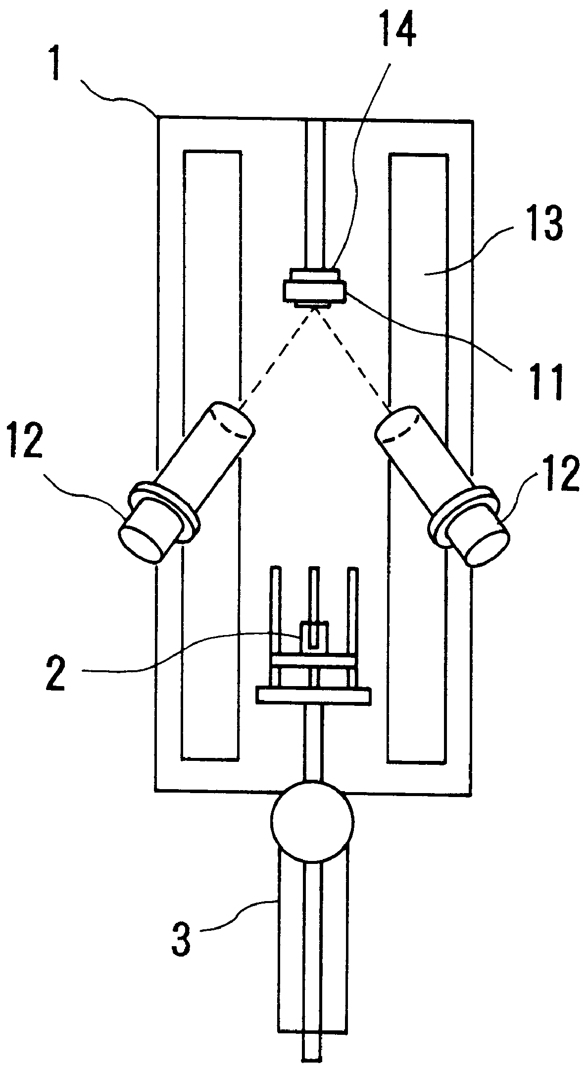
Ga crystals were made to grow on a GaAs (001) substrate using the crystal growth observing apparatus with the structure mentioned above.

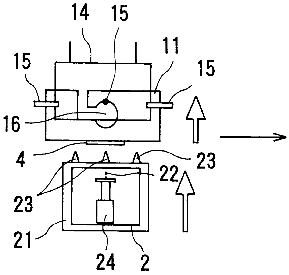
The STM (2) was housed in the lower portion of the MBE device (1) by the STM drive mechanism (3) and a GaAs buffer was made to grow by the MBE growing method after cleaning the surface of the GaAs substrate.

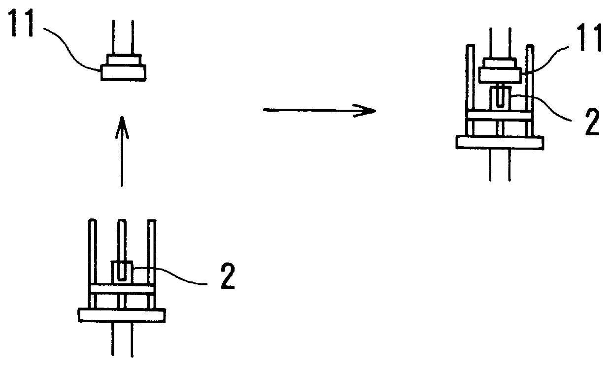
The STM was moved upward with the temperature of the substrate (4) preserved and the substrate holder (11) was lifted while catching the substrate holder (11) by the projections (23) at three positions opposed to the substrate holder (11).

The substrate holder (11) was separated from the substrate heating mechanism (14) and was itself incorporated with the STM (2) through the wide clearance formed between the substrate holder (11) and the substrate heating mechanism (14).

The STM probe (22) was moved into contact with the surface of the substrate (4). A STM observation mode was prepared.

Subsequently, raw materials in the amount of which an atomic l...


PUM

PropertyMeasurementUnit
diameteraaaaaaaaaa
scanning tunneling microscopeaaaaaaaaaa
vapor pressureaaaaaaaaaa

Abstract

A STM drive mechanism capable of moving a scanning tunneling microscope (STM) incorporated with a molecular beam epitaxy (MBE) device in the MBE device under vacuum and a substrate holder with a wide clearance formed between a substrate heating system and the substrate holder are provided. The STM is protected by a heat insulating shield from high vapor pressure atmosphere and radiant heat according to substrate heating.

Description

The present invention relates to a crystal growth observing apparatus. More particularly, the present invention relates to a crystal growth observing apparatus which permits observation of crystal growth at a stare where a crystal(s) is growing.DESCRIPTION OF THE PRIOR ARTWith respect to crystal growth, observation in the growing process is one of the most important matters. Since uniformity of growth at the atomic level is particularly required in the quantum nano structure which has recently been attracted, an observing technique at a state where a crystal(s) is growing is needed.For example, a reflecting high-speed electron beam diffraction method and a reflectance difference spectral method have already been put into practice for the crystal growth by the molecular beam epitaxy (MBE) and permit real-time observation of crystal growth.These conventional methods of observing crystal growth only permit average estimation of real spaces at levels more than the micro one, but cannot ...

Claims


Application Information

Patent Timeline
Patent Type & Authority Patents(United States)
IPC IPC(8): C30B23/02B05C11/00G01N37/00C30B23/08G01N27/00G01Q30/18G01Q30/20G01Q60/10G01Q80/00H01L21/203
CPCB82Y35/00C30B23/02G01Q60/16G01Q30/02Y10T117/1004Y10S977/852
Inventor TSUKAMOTO, SHIROKOGUCHI, NOBUYUKI
Owner NATIONAL RESEARCH INSTITUTE FOR METALS SCIENCE AND TECHNOLOGY AGENCY
Why Eureka
Try Eureka