Method for forming a self-aligned contact

a self-aligning, contact technology, applied in the direction of semiconductor/solid-state device manufacturing, basic electric elements, electric devices, etc., can solve the problems of short circuit, current leakage, short circuit in the device,

Inactive Publication Date: 2000-07-04
UNITED MICROELECTRONICS CORP
View PDF6 Cites 50 Cited by
  • Summary
  • Abstract
  • Description
  • Claims
  • Application Information

AI Technical Summary

Problems solved by technology

The improper electrical coupling usually causes a short circuit in the device.
When the misaligned contact opening is filled with metallic material, the interchangeable source / drain and the gate structure are improperly coupled, resulting in a short circuit.
In this structure, a stress consequently exits between the spacer made of silicon nitride and the gate, causing a defect of the gate, and further resulting in a current leakage.

Method used


Image

  • Method for forming a self-aligned contact
  • Method for forming a self-aligned contact
  • Method for forming a self-aligned contact

Examples


Embodiment Construction

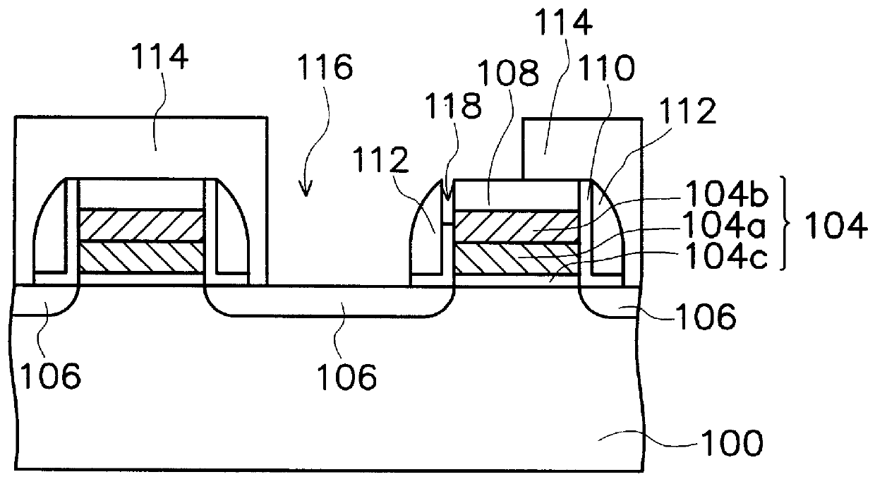
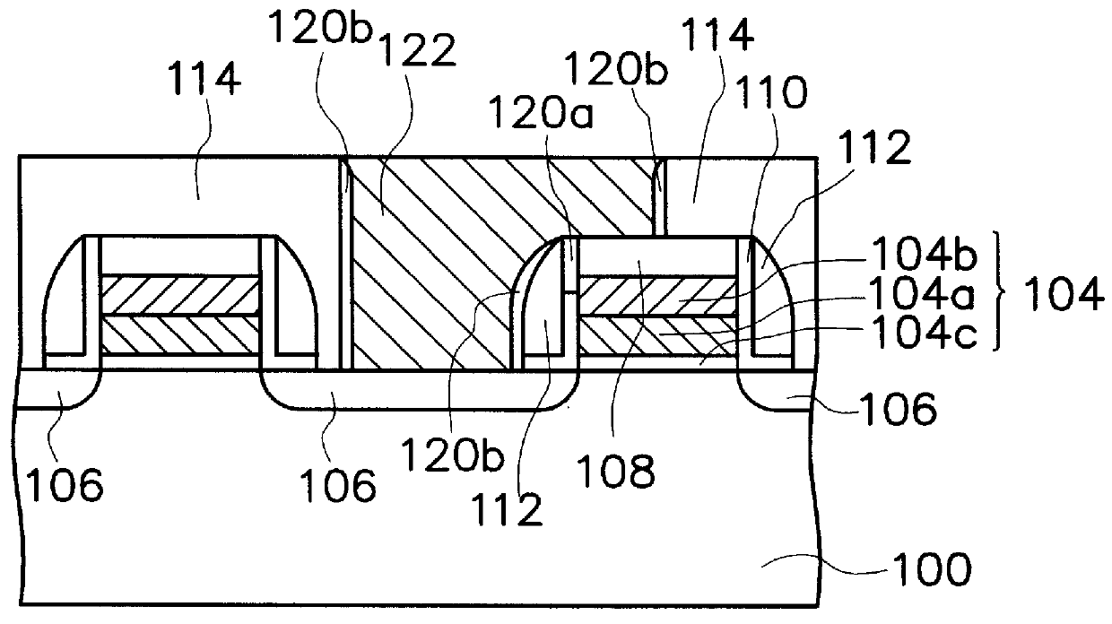
The conventional process to form a self-aligned contact (SAC) opening has a short circuit issue due to a clearance between a spacer and a gate. The invention introduces an additional process to fill the clearance with insulating material so as to fully isolate the gate. There is no short circuit occurring in the invention. Detail descriptions, according to the invention, are following.

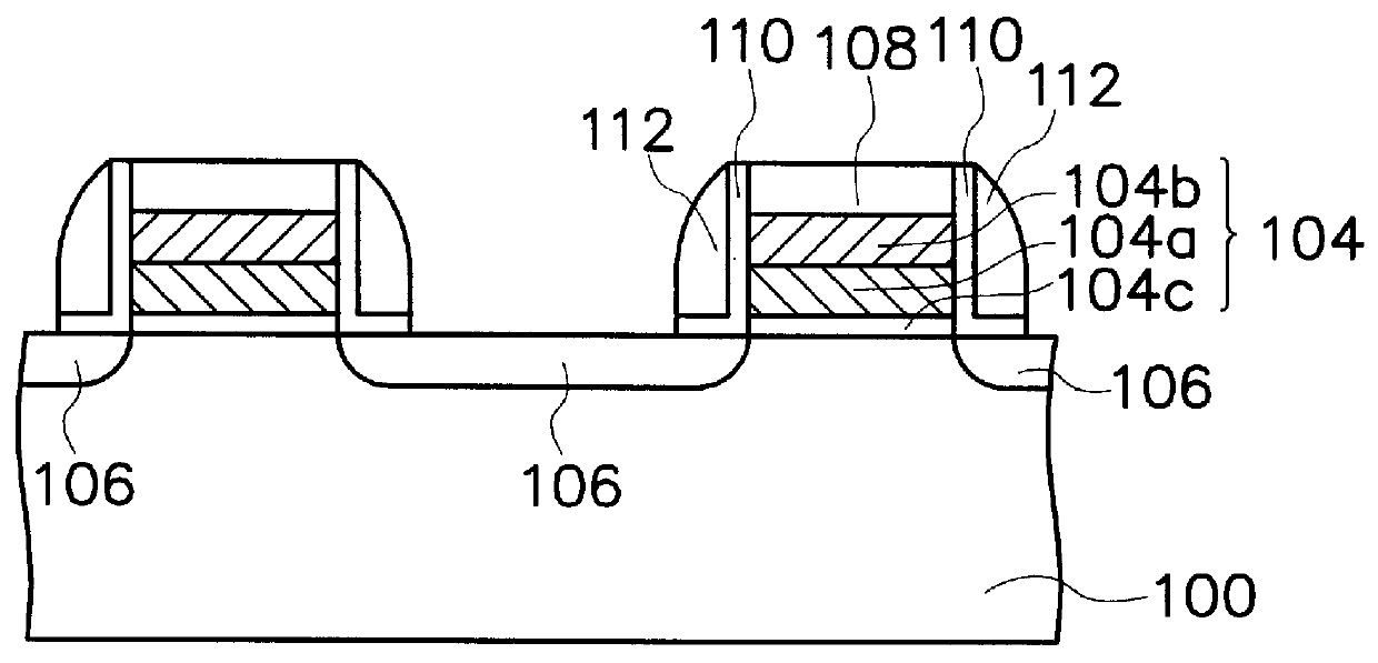
FIGS. 1A-1D are cross-sectional view of a portion of a substrate, schematically illustrating a fabrication process to form a self-aligned contact opening to expose an interchangeable source / drain region. In FIG. 1A, a gate structure 104 is formed on a semiconductor substrate 100, and a junction region 106, which is a source region or a drain region. The gate structure 104 further includes a gate oxide layer 104c, a polysilicon layer 104a, and a metal silicide layer 104b. A cap layer 108 including, for example, silicon nitride is formed on the gate structure 104. A liner oxide layer 110 and a spacer 112...


PUM


Abstract

A method for forming a SAC opening is provided. As a self-aligned contact (SAC) opening is formed in a dielectric layer on a semiconductor substrate to expose one of source/drain regions in the substrate, a misalignment of the SAC opening may occur to expose a portion of the gate structure. The gate structure has a gate, which is covered by a cap layer on the top, a thin oxide layer on each sidewall of the gate and the cap layer, and a spacer on the thin oxide layer. The SAC opening causes a clearance between the spacer and the gate since a portion of the thin oxide layer is removed. The method contains forming an insulating layer over the substrate to fill the clearance. An etching back process is performed to remove the insulating layer so that a remaining portion of the insulating layer fills the clearance to fully isolate the gate.

Description

This application claims the priority benefit of Taiwan application serial no. 88101 194, filed Jan. 27, 1999, the full disclosure of which is incorporated herein by reference.1. Field of the InventionThis invention relates to semiconductor fabrication, and more particularly to a method form forming a self-aligned contact (SAC).2. Description of Related ArtAs semiconductor device integration continuously increases, the device dimension is necessary to be accordingly reduced. Thus, a contact opening in the device needs a more precise alignment to prevent an improper electrical coupling to the adjacent device element from occurring as an metallic material is filled into the contact opening. The improper electrical coupling usually causes a short circuit in the device. For example, a contact opening is desired to expose a interchangeable source / drain region but it may also expose a portion of a gate structure if a misalignment occurs. When the misaligned contact opening is filled with m...

Claims


Application Information

Patent Timeline
Patent Type & Authority Patents(United States)
IPC IPC(8): H01L21/60H01L21/02
CPCH01L21/76897
Inventor LIN, KWANG-MINGCHEN, RUSSELL
Owner UNITED MICROELECTRONICS CORP
Why Eureka
Try Eureka