
Solder ball arrangement device

Inactive Publication Date: 2000-08-01
NEC CORP
View PDF15 Cites 25 Cited by
  • Summary
  • Abstract
  • Description
  • Claims
  • Application Information

AI Technical Summary

Problems solved by technology

The conventional solder ball transfer device has, however, a problem in that the complicated structure of the holes 32a and associated slots 32b in the alignment plate 32 raises the cost of the device, especially in the case of a high density ball pattern such as having a small pitch as low as 300 .mu.m with a large number of pads as high as 2000.
If the alignment plate is formed by an etching technique for achieving the high density, the alignment plate will suffer from lack of mechanical strength due to a small thickness thereof.

Method used


Image

  • Solder ball arrangement device
  • Solder ball arrangement device
  • Solder ball arrangement device

Examples


Embodiment Construction

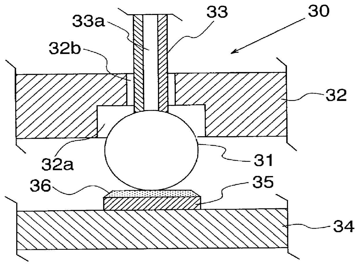
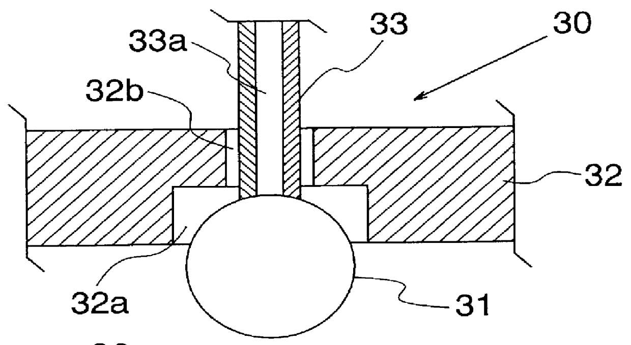
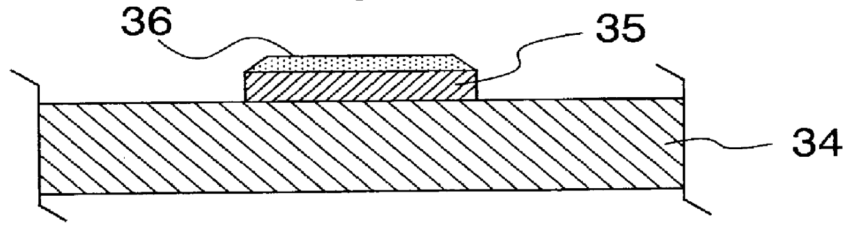
Now, the present invention is more specifically described with reference to accompanying drawings. Referring to FIG. 2, a solder ball arrangement device 11 according to a first embodiment of the present invention comprises an arrangement plate 13 having therein an array of through-holes 13a having a tapered inner surface, a porous member 15 made of a porous material and bonded to the arrangement plate 13, and a housing member 14 for receiving the arrangement plate 13 and the porous member 15, with an air space 14a left below the bottom of the porous member 15. The housing member 14 has a nozzle or air outlet 14b communicated with the air space 14a. A vacuum pump not shown in the figure is connected to the nozzle 14b of the housing member 14 for suction of air from the air space 14a. Each through-hole 13a of the arrangement plate 13 can receive therein a solder ball 12 and has a truncated pyramid shape, the larger bottom of which is directed upward during arrangement of the solder ba...


PUM

PropertyMeasurementUnit
Diameteraaaaaaaaaa
Shapeaaaaaaaaaa
Permeabilityaaaaaaaaaa

Abstract

A solder ball arrangement device has a thin arrangement plate having a plurality of through-holes of a truncated pyramid shape, a porous member bonded to the arrangement plate, and a housing member for receiving the arrangement plate and the porous member for defining an air space inside the housing member. A suction pump is provided to evacuate the air space and to receive an array of solder balls in the through-holes by suction. The through-holes are formed by etching, and the porous member reinforces the thin arrangement plate.

Description

(a) Field of the InventionThe present invention relates to a solder ball arrangement device and, more particularly, to a solder ball arrangement device for use in transferring an array of solder balls onto a mounting board to form an array of bump electrodes in a BGA (ball grid array) technique, a CSP (chip size package) technique, or a flip chip bonding technique. The present invention also relates to a method for fabrication thereof.(b) Description of the Related ArtBump electrodes formed by a BGA technique, a CSP technique, and a flip chip bonding technique are increasingly used in mounting a semiconductor chip onto a mounting board. In the recent advance of semiconductor integrated circuits, a large number of external pins are disposed at a smaller pitch, with increased mounting density, reduced device area and increased capacity of the integrated circuits. In the method for forming bump electrodes by using metallic solder balls, it is especially important to arrange a large num...

Claims


Application Information

Patent Timeline
IPC IPC(8): B23K3/06B23K35/02H01L21/48H01L21/60H01L21/02H05K3/34H05K13/02
CPCB23K3/0623B23K35/0244H01L21/4853H01L24/11H05K3/3478B23K2201/40H01L2224/13099H01L2924/01004H01L2924/01013H01L2924/14H05K2201/0116H05K2203/041H05K2203/082H01L2224/11003H01L2224/11334H01L2924/01005H01L2924/01006H01L2924/01033H01L2924/014B23K2101/40H05K3/3436H05K3/0094H05K2201/10734
Inventor TAKAHASHI, NOBUAKISENBA, NAOJISHIMADA, YUZO
Owner NEC CORP
Learn More