Method of making ultra thin gate oxide using aluminum oxide

a gate oxide and aluminum oxide technology, applied in the field of semiconductor processing, can solve the problems of increasing the potential for reliability problems associated with dielectric breakdown and hot and cold carrier injection degradation, and the introduction of a new set of silicon dioxide layers

Inactive Publication Date: 2000-08-08
GLOBALFOUNDRIES INC
View PDF3 Cites 28 Cited by
  • Summary
  • Abstract
  • Description
  • Claims
  • Application Information

AI Technical Summary

Problems solved by technology

However, the scaling of silicon dioxide gate dielectric layers has introduced another set of problems.
To begin with, very thin silicon dioxide layers have been historically difficult to fabricate with a consistent thickness across a given wafer, from wafer to wafer and from lot to lot.
In addition, as the thickness of silicon dioxide is scaled downward, the potential for reliability problems associated with dielectric breakdown and hot and cold carrier injection degradation increases.
Hot and cold carrier degradation can significantly reduce device performance, while dielectric breakdown can lead to complete device failure.
One potential cause of carrier injection and potential dielectric breakdown is thought to occur as a result of interface traps near the Si--SiO.sub.2 interface.
Independent of the exact physical cause of carrier injection, the empirical result for very thin oxides may be gate leakage currents and / or catastrophic device failure.
Another difficulty associated with very thin conventional gate oxides is polysilicon depletion.
If the amount of boron diffused is sufficiently high, the electrical performance of the field effect transistor may be severely degraded due to polysilicon depletion.

Method used


Image

  • Method of making ultra thin gate oxide using aluminum oxide
  • Method of making ultra thin gate oxide using aluminum oxide
  • Method of making ultra thin gate oxide using aluminum oxide

Examples


Embodiment Construction

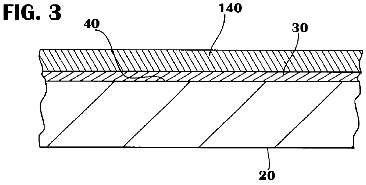
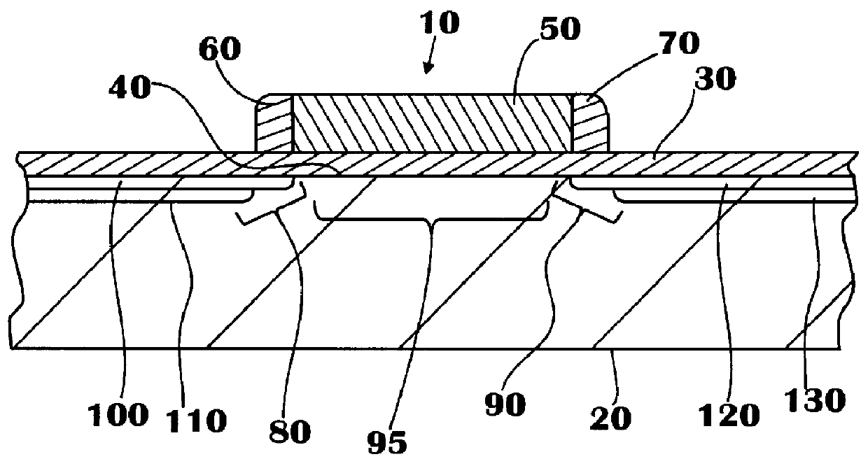
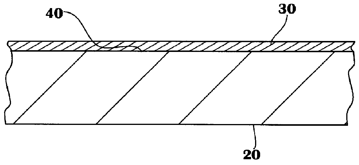
In the drawings described below, reference numerals are generally repeated where identical elements appear in more than one figure. Turning now to the drawings, and in particular to FIG. 1, there is shown a cross-sectional view of an exemplary embodiment of a transistor 10 that is formed on a semiconductor substrate 20. The semiconductor substrate 20 may be composed of n-doped, or p-doped silicon, silicon-on-insulator, or other suitable substrate materials. The transistor 10 includes an insulating or gate dielectric layer 30 that is formed on the upper surface 40 of the substrate 20 and a gate electrode 50 that is formed on the first insulating layer 30. Dielectric sidewall spacers 60 and 70 are positioned adjacent the gate electrode 50. Source / drain regions 80 and 90 are formed in the substrate 20 and laterally separated to define a channel region 95 beneath the gate electrode 50. The source / drain region 80 includes a lightly doped drain ("LDD") region 100 and a partially overlappi...


PUM

PropertyMeasurementUnit
thickaaaaaaaaaa
thickaaaaaaaaaa
thicknessaaaaaaaaaa

Abstract

A transistor and a method of making the same are provided. The method includes the step of forming a gate dielectric layer on the substrate where the gate dielectric layer is composed of an aluminum oxide containing material. A gate electrode is formed on the gate dielectric layer and first and second source/drain regions are formed in the substrate laterally separated to define a channel region beneath the gate electrode. The aluminum oxide containing material may be, for example, Al2O3. Aluminum oxide provides for a gate dielectric with a thin equivalent thickness of oxide in a potentially single crystal form.

Description

1. Field of the InventionThis invention relates generally to semiconductor processing, and more particularly, to a transistor with an aluminum oxide containing gate dielectric layer, and to a method of making the same.2. Description of the Related ArtA conventional field effect transistor implemented in silicon typically consists of a source and a drain formed in a silicon substrate, and separated laterally to define a channel region in the substrate. A gate dielectric layer is positioned on the substrate over the channel region and a gate electrode composed of a conducting material, such as aluminum or doped polysilicon, is disposed on the gate dielectric layer. The gate electrode is designed to emit an electric field into the channel region. Changes in the electric field emitted by the gate electrode enable, or alternatively, disable the flow of current between the source and the drain.In a conventional process flow for forming a typical field effect transistor, a gate oxide layer...

Claims


Application Information

Patent Timeline
Patent Type & Authority Patents(United States)
IPC IPC(8): H01L21/02H01L21/28H01L29/51H01L21/336H01L29/40
CPCH01L21/28185H01L29/517H01L29/6659H01L21/28194
Inventor GARDNER, MARK I.GILMER, MARK C.SPIKES, JR., THOMAS E.
Owner GLOBALFOUNDRIES INC
Why Eureka
Try Eureka