Process for reducing surface roughness of superconductor integrated circuit having a ground plane of niobium nitride of improved smoothness

a technology of niobium nitride and integrated circuit, which is applied in the direction of superconductor devices, solid-state devices, coatings, etc., can solve the problems of unacceptably high inductance of nbn/mgo/nbn devices between nbn/mgo/nbn trilayer devices, increased parasitic inductance, and so on

Inactive Publication Date: 2000-08-29
NORTHROP GRUMAN CORP
View PDF1 Cites 13 Cited by
  • Summary
  • Abstract
  • Description
  • Claims
  • Application Information

AI Technical Summary

Problems solved by technology

While the use of bias sputtered SiO.sub.2 effectively smooths the surface roughness of a NbN ground plane to enable the fabrication of high current density NbN / MgO / NbN trilayer devices over the thick NbN ground plane, there still exists a problem that this process produces NbN / MgO / NbN devices with unacceptably high inductance existing between the NbN / MgO / NbN trilayer devices and the ground plane which is the result of the layer of SiO.sub.2 spacing the NbN / MgO / NbN trilayer devices from the ground plane.
In FIG. 1, the trilayer devices 10 are spaced approximately 150 nm away from the ground plane 22 which spacing is sufficient to effectively prevent excessive leakage or even short circuits but results in the aforementioned increased parasitic inductance.
This surface roughness is so great that either excessive leakage or short circuits would result if the trilayer devices 10 were fabricated directly on the NbN ground plane 23.
The resultant product is not sufficiently smooth to permit fabrication of circuits requiring smoothness on the order of that required to permit NbN / MgO / NbN trilayer devices to be directly formed on a NbN ground plane.
Single crystal NbN can be made smooth but large scale fabrication useful for integrated circuits is difficult to achieve because of many surface defects which make the resultant NbN / MgO / NbN trilayer junctions inoperative.
However, niobium titanium nitride is subject to high stress making it unusable for NbN / MgO / NbN trilayer devices having a ground plane for reducing parasitic inductance.

Method used


Image

  • Process for reducing surface roughness of superconductor integrated circuit having a ground plane of niobium nitride of improved smoothness
  • Process for reducing surface roughness of superconductor integrated circuit having a ground plane of niobium nitride of improved smoothness
  • Process for reducing surface roughness of superconductor integrated circuit having a ground plane of niobium nitride of improved smoothness

Examples


Embodiment Construction

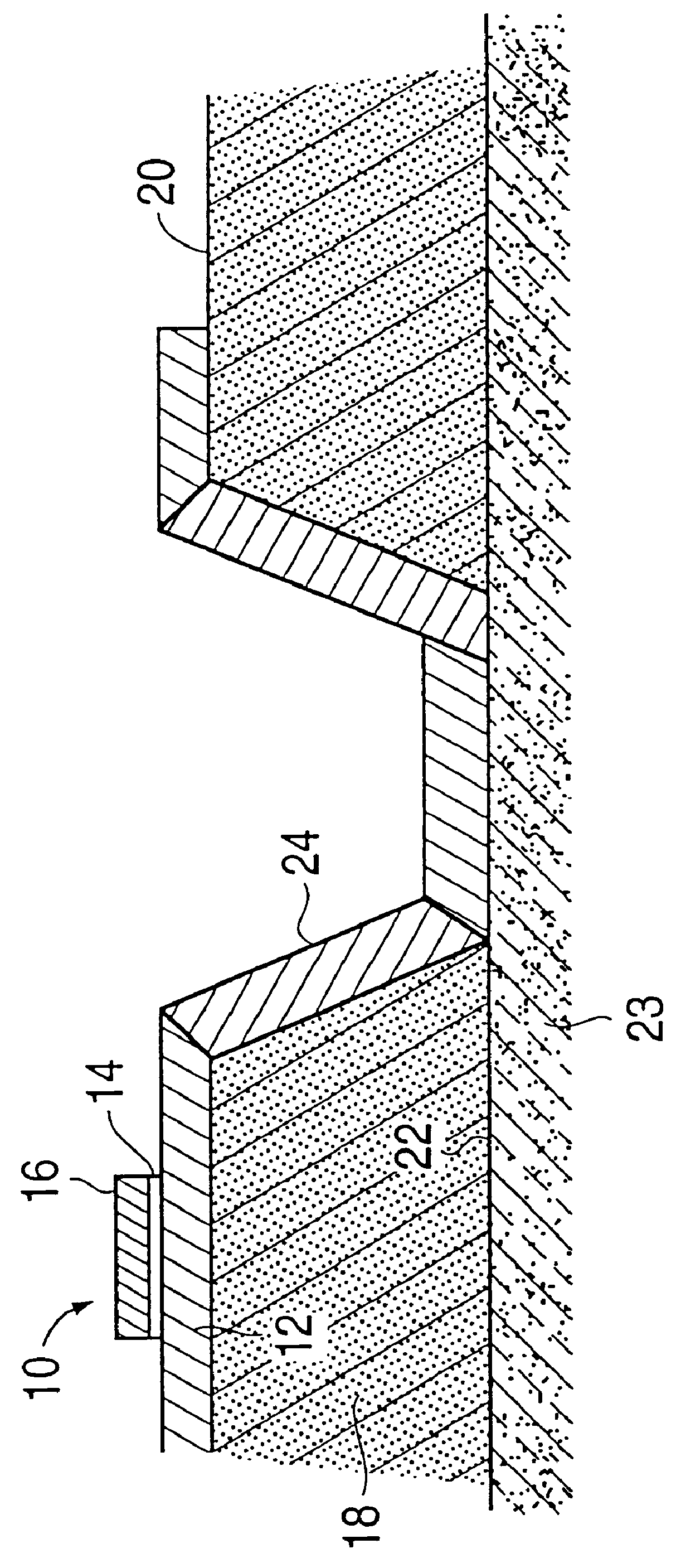
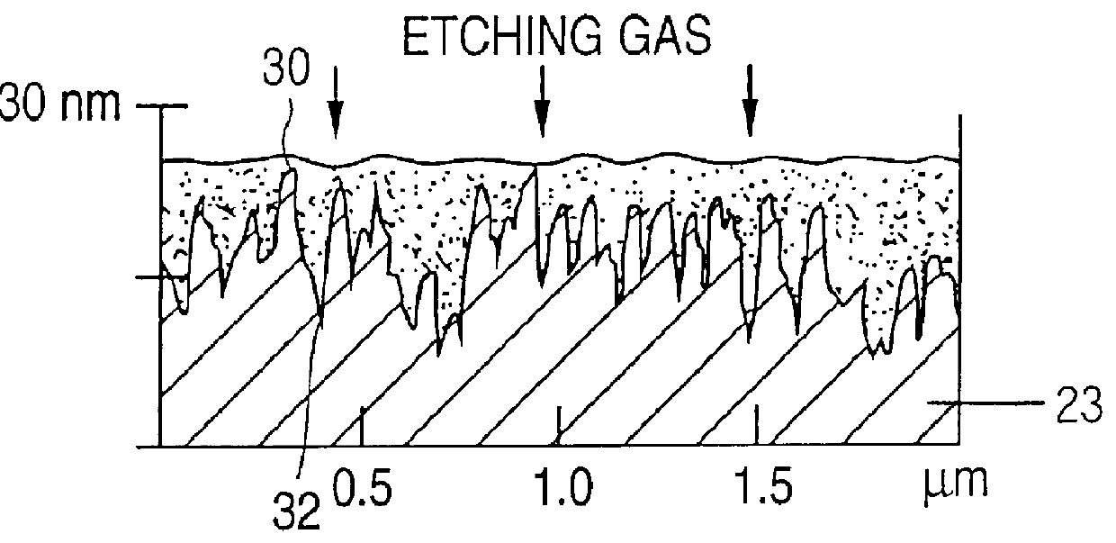
A process for reducing roughness on a surface of superconductor material, such as NbN, in accordance with the invention is illustrated in FIGS. 2-5. The starting point for the process is the prior art NbN substrate of FIG. 2. The NbN substrate (ground plane), as illustrated in FIG. 2, has peaks 30 and valleys 32 which vary between 15 and 20 nm in depth (over 4 nm rms) making it impossible to form a NbN / MgO / NbN trilayer device directly on the top surface of the substrate because of the unacceptable roughness of the top surface of the NbN.

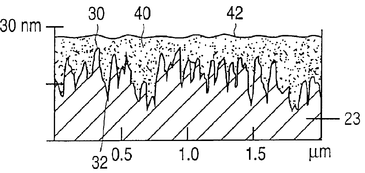
The present invention modifies the above described prior art processing of the NbN ground plane as discussed above and described in the aforementioned pending patent applications and publication by smoothing the top surface of the thick NbN ground plane sufficiently (less than 1 nm rms) to permit direct fabrication of the NbN / MgO / NbN trilayer devices on the NbN substrate. An oxide layer 40, as illustrated in FIG. 3, is directly formed on the rough to...


PUM

PropertyMeasurementUnit
thicknessaaaaaaaaaa
thicknessaaaaaaaaaa
surface roughnessaaaaaaaaaa

Abstract

The invention is a process for reducing roughness of a surface of a superconductor material (23) having an undesirable surface roughness (30 and 32) and a trilayer superconductor integrated circuit (100). The process for reducing roughness of a surface of superconductor material having an undesirable surface roughness includes coating the surface with an oxide layer (40) to fill the undesirable surface roughness and to produce an exposed oxide surface (42) with a roughness less than the surface roughness; and etching the exposed oxide surface to remove a thickness of the oxide layer followed by removing at least a portion of the oxide layer filling the undesirable surface roughness and a portion of the surface of the superconductor material to produce an exposed etched surface (44) comprised of at least the superconductor material which has a surface roughness less than the undesirable surface roughness.

Description

Field of the InventionThe present invention relates to processes for reducing surface roughness of superconductor and semiconductor materials and more particularly, to processes for reducing the surface roughness of niobium nitride (NbN) and to superconductor integrated circuits formed on a ground plane of NbN.DESCRIPTION OF THE PRIOR ARTSuperconductor integrated circuits utilizing NbN ground plane have been developed which operate at 10 K. These circuits utilize a thick (500 nm) NbN ground plane layer disposed on thermally oxidized silicon wafers and trilayer Josephson junction for the active device. The thick NbN layer has a high surface roughness which prevents direct fabrication of trilayer devices on the top surface thereof as described below in more detail in conjunction with FIG. 2Superconductor niobium nitride integrated circuits having NbN / MgO / NbN trilayer devices have substantial high current density tunnel junctions ranging from 1,000 A / cm.sup.2 to 5,000 A / cm.sup.2. See G...

Claims


Application Information

Patent Timeline
Patent Type & Authority Patents(United States)
IPC IPC(8): H01L39/24H01L27/18
CPCH01L27/18H01L39/2416Y10S505/731Y10S505/82H10N69/00H10N60/12H10N60/0241
Inventor KERBER, GEORGE L.LEUNG, MICHAEL
Owner NORTHROP GRUMAN CORP
Why Eureka
Try Eureka