Via pad geometry supporting uniform transmission line structures

a transmission line and geometry technology, applied in the direction of electrical apparatus construction details, orthogonal pcbs mounting, printed element electric connection formation, etc., can solve the problems of difficult circuit board manufacturing, degrading the quality of the signal being transmitted, and significant interference effects

Inactive Publication Date: 2000-08-29
INTEL CORP
View PDF4 Cites 36 Cited by
  • Summary
  • Abstract
  • Description
  • Claims
  • Application Information

AI Technical Summary

Problems solved by technology

As this frequency increases, interference effects become significant.
In particular, high frequency signals are reflected by variations in the impedance of a trace, degrading the quality of the signal being transmitted.
These vias typically have large diameters relative to the signal and reference traces because it is difficult to manufacture circuit boards with small diameter vias.
In such closely packed configurations, the relatively large via diameters can obstruct the most direct path between the devices, forcing the signal traces to be routed around the vias.
The resulting variation in the impedance of the signal trace increases the signal degradation due to interference effects.
These impedance variations and the consequent interference arise, for example, with memory devices such as those designed by Rambus Corporation of Mountain View, Calif.
The signal traces must be routed around vias and coupled to device pads, altering the trace impedance and generating interference-induced noise on the signal traces.

Method used


Image

  • Via pad geometry supporting uniform transmission line structures
  • Via pad geometry supporting uniform transmission line structures
  • Via pad geometry supporting uniform transmission line structures

Examples


Embodiment Construction

The following description sets forth numerous specific details to provide a thorough understanding of the invention. However, those of ordinary skill in the art having the benefit of this disclosure will appreciate that the invention may be practiced without these specific details. In other instances, well known methods, procedures, components, and circuits have not been described in detail in order to more clearly highlight the features of the present invention.

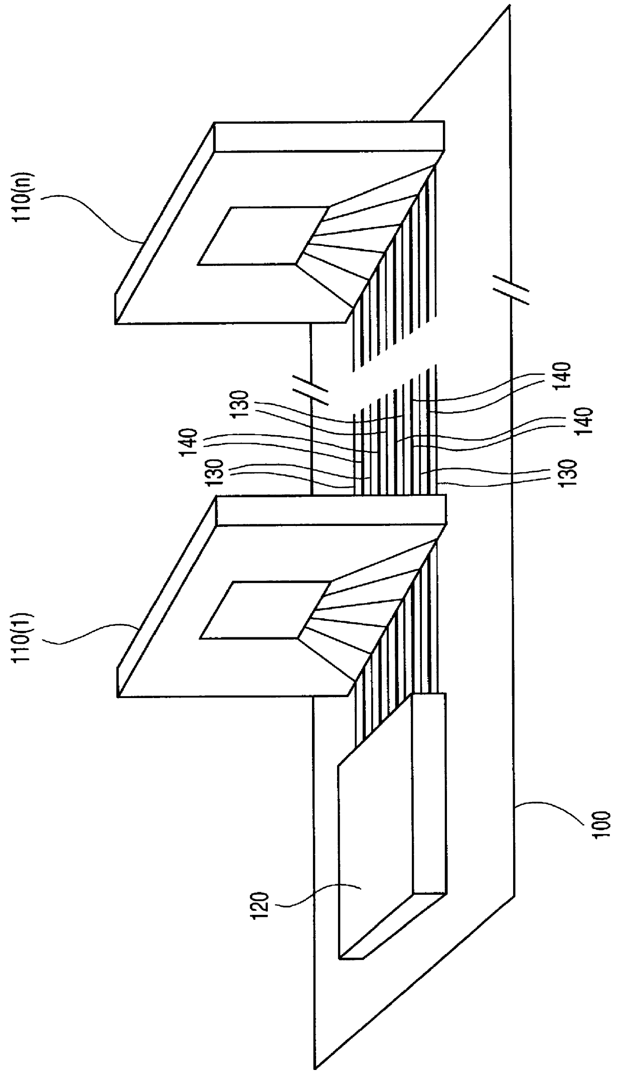
The present invention is described with reference to memory devices, such as those designed by Rambus Corporation of Mountain View, Calif., and the coupling of these devices to a memory controller associated with a microprocessor or similar device. It is understood that the present invention may be employed advantageously wherever spatial and timing constraints require routing high frequency signals in closely spaced configurations.

Interference effects, such as those noted above, are becoming prevalent at the system level, w...


PUM


Abstract

A connector for coupling high frequency signals between devices includes a substrate having an array of vias for coupling a reference voltage to reference voltage traces that extend along the substrate surface between the devices. Signal traces including device pads for coupling signals to and from the devices alternate with the reference voltage traces. The widths of the reference voltage traces are varied to maintain a substantially constant separation between the reference voltage trace and an adjacent signal trace.

Description

1. Technical FieldThis invention relates to the field of electrical interconnects, and in particular to electrical interconnects for high frequency signals.2. Background ArtThe core operating frequencies of microprocessors have been increasing steadily, and it is expected that processors operating in the gigahertz (GHz) frequency regime will soon be available. In order to take full advantage of the speed of these microprocessors, computer systems must be able to couple data to and from the microprocessor core at ever increasing rates. The data transfer rate is typically increased by increasing the frequency at which signals are driven onto the traces that couple data between the processor and associated devices such as memory modules. As this frequency increases, interference effects become significant. In particular, high frequency signals are reflected by variations in the impedance of a trace, degrading the quality of the signal being transmitted. These impedance variations are a...

Claims


Application Information

Patent Timeline
Patent Type & Authority Patents(United States)
IPC IPC(8): H05K1/11H05K1/02H05K3/42
CPCH05K1/0219H05K1/116H05K3/429H05K2201/044H05K2201/09236H05K2201/09381H05K2201/09727
Inventor LEDDIGE, MICHAELSPRIETSMA, JOHN
Owner INTEL CORP
Why Eureka
Try Eureka