

Self-aligned contact process using low density/low k dielectric
- Summary
- Abstract
- Description
- Claims
- Application Information
AI Technical Summary
Problems solved by technology
Method used
Image

Examples
Embodiment Construction
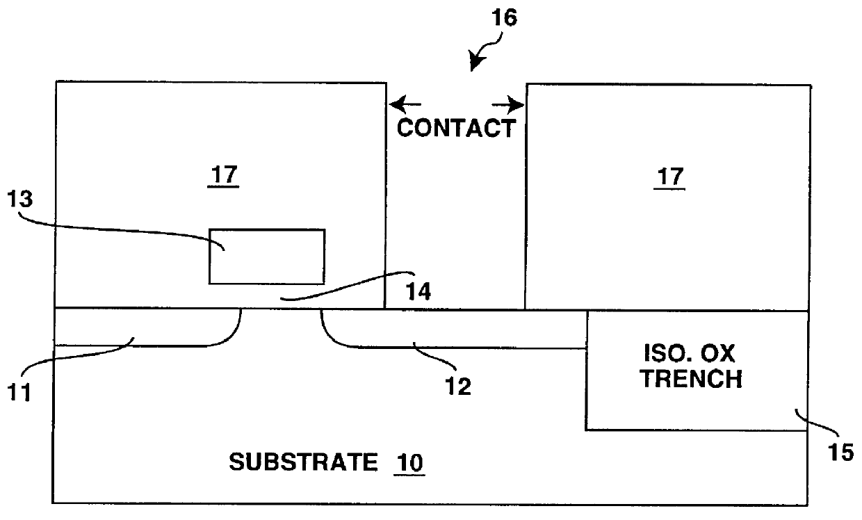
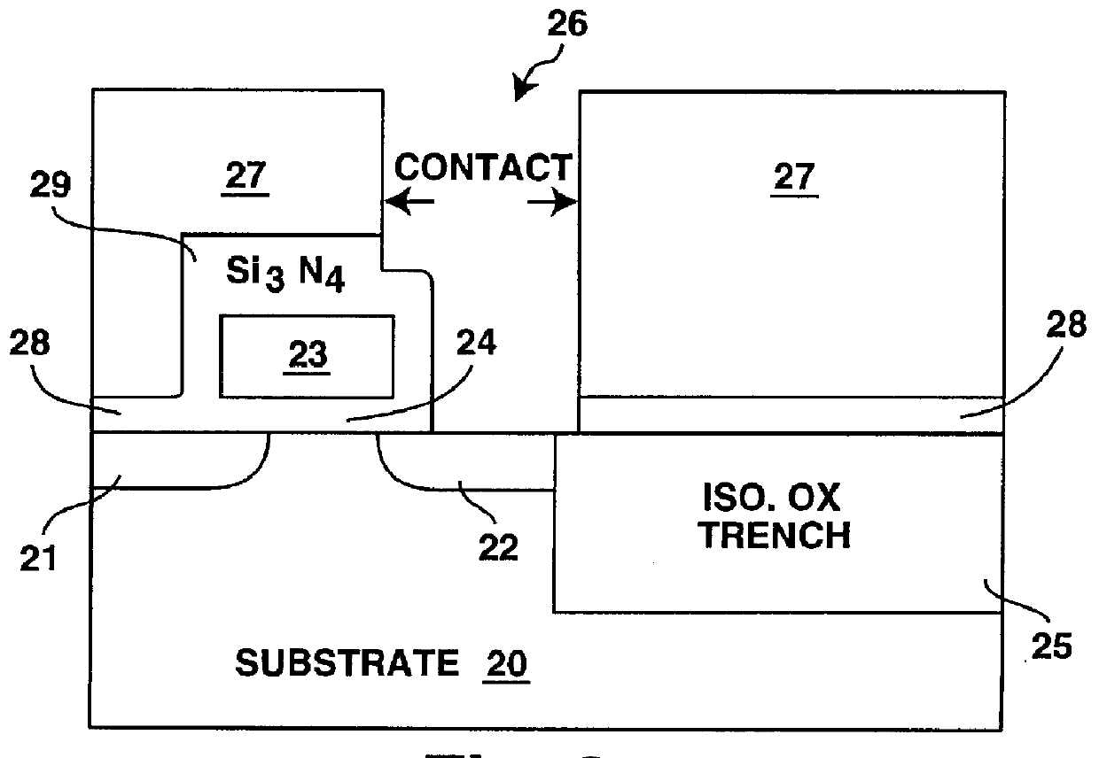
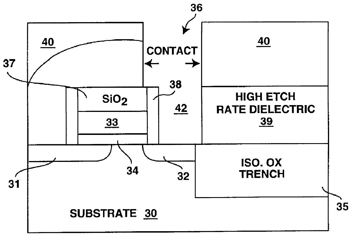
A method and apparatus is disclosed for an unlanded contact to a substrate for use in an MOS field-effect transistor. In the following description, numerous specific details are set forth such as specific materials, in order to provide a thorough understanding of the present invention. It will be apparent, however, that the present invention may be practiced without these specific details. In other instances, well-known steps such as doping steps used to form the source and drain regions of field-effect transistors are not described in detail in order not to obscure the present invention.
In the cross-sectional elevation view of FIG. 3, a contact 42 is illustrated in an opening 36 which contacts the doped region 32 of the substrate 30. As will be seen from FIGS. 4-7, the unlanded contact 42 is achievable with the present invention in part through use of low k and / or low density dielectric materials with etch rates much higher than silicon dioxide and silicon nitride.
An ordinary monoc...
PUM
 Abstract
Description
Claims
Application Information