Bist architecture for detecting path-delay faults in a sequential circuit

a sequential circuit and path-delay technology, applied in the direction of electronic circuit testing, measurement devices, instruments, etc., can solve the problems of physical defects in the circuit, failures may occur during manufacturing, and the generation of the necessary test patterns to stimulate the circuit becomes increasingly complex

Inactive Publication Date: 2000-11-14
LUCENT TECH INC +1
View PDF14 Cites 92 Cited by
  • Summary
  • Abstract
  • Description
  • Claims
  • Application Information

AI Technical Summary

Problems solved by technology

Faults may occur during manufacturing or over time as a result of wearout.
Structural faults represent a physical defect in the circuit.
As the complexity and size of the circuit increases, the generation of the necessary test patterns to stimulate the circuit also becomes increasingly more complex.
Although it is relatively simple to generate test patterns for detecting faults in a combinational circuit, significantly more complex test vectors are required to detect faults in a sequential circuit because of the need to propagate known values from element to element over time.
Path-delay faults can arise from both manufacturing process parameter variations as well as spot defects in a circuit.
Thus, detection of path-delay faults requires stricter justification and propagation conditions and, as a result, such faults are more difficult to detect using the random test vectors employed for stuck-at faults.
Conventional test pattern generators for stuck-at faults are thus unsuitable for path-delay faults in which a correlation exists between successively generated test vectors.
As a result, the partial scan-based BIST architecture disclosed in U.S. Pat. No. 5,329,533 for detecting stuck-at faults cannot be used to test for path-delay faults.
The method and apparatus described in that patent, however, is only suitable for path-delay fault testing of combinational circuits which, unlike sequential circuits, have very little practical industrial use.

Method used


Image

  • Bist architecture for detecting path-delay faults in a sequential circuit
  • Bist architecture for detecting path-delay faults in a sequential circuit
  • Bist architecture for detecting path-delay faults in a sequential circuit

Examples


Embodiment Construction

In the description of the invention the terms "high" and "one" are used interchangeably to denote a digital logic value "1"while the terms "low" and "zero" are used interchangeably to denote a digital logic value "0".

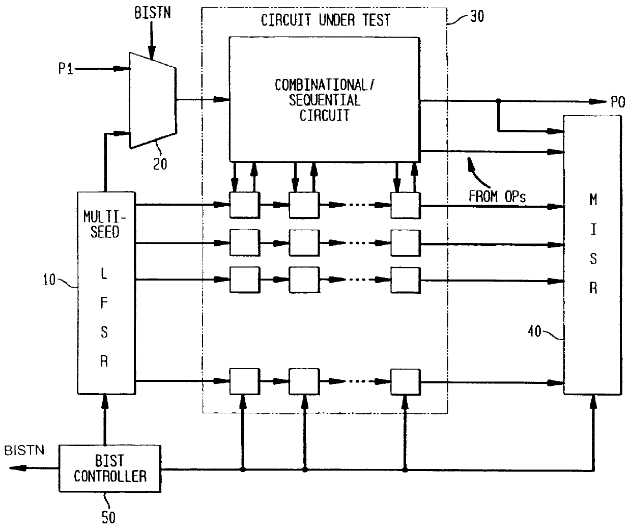
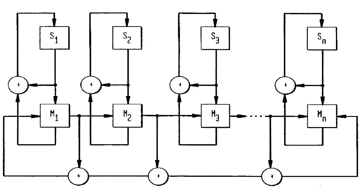
The present invention provides an apparatus for detecting path-delay faults and stuck-at faults in a sequential circuit that has been converted into a combinational circuit (full scan) or a less complex sequential circuit (partial scan), using a modified form of the scan-based BIST architecture described in U.S. Pat. No. 5,329,533 which, as pointed out above, is suitable only for the detection of stuck-at faults. The inventive arrangement is similar to that disclosed in U.S. Pat. No. 5,329,533 except for the test pattern generator and different test controller that employs a different clocking scheme that is applied during the test application mode. As discussed above, path-delay fault testing requires a pair of test patterns. Thus, the inventive scan-based BIST archite...


PUM


Abstract

A scan-based BIST architecture for detecting path-delay faults in a sequential circuit converted to a combinational circuit or a less complex sequential circuit including a combinational portion and a plurality of scan flip-flops. The BIST structure includes a test pattern generator for generating two test patterns and a controller for generating a clock signal and an extended scan mode signal which is held high for two clock cycles while the output response of the combinational portion to the first and second test vectors is latched into the scan flip-flops in order to detect a signal transition. The invention is further directed to a method for detection of path-delay faults using this scan-based BIST architecture. To improve the fault coverage for path-delay faults, observation points may be inserted at the inputs of selected scan flip-flops. A predetermined number of scan flip-flops having the highest activation frequency are selected as the observation points.

Description

1. Field of the InventionThe present invention relates to a device and method for detecting path-delay faults in a sequential circuit. In particular, the invention provides a clocking scheme for use with a scan-based built-in self-test (BIST) architecture to detect path-delay faults in a sequential circuit and a technique for selecting observation points to improve fault coverage.2. Description of the Related ArtIntegrated circuits comprise one or more individual circuit elements, each of which is either combinational, e.g. a logic gate, or sequential, e.g. a flip-flop. It is beneficial to evaluate a circuit to ensure that it is fault-free. Faults may occur during manufacturing or over time as a result of wearout. Testing of the circuit results in a fault coverage ratio that represents the ratio of faults that can be detected to all faults which are taken into consideration, expressed as a percentage. Fault coverage values range between an ideal value of 100%, where all faults are d...

Claims


Application Information

Patent Timeline
Patent Type & Authority Patents(United States)
IPC IPC(8): G01R31/3185G01R31/30G01R31/28
CPCG01R31/31858G01R31/3016
Inventor BHAWMIK, SUDIPTACHAKRABORTY, TAPAN JYOTIMUKHERJEE, NILANJAN
Owner LUCENT TECH INC
Why Eureka
Try Eureka