Layout for semiconductor memory including multi-level sensing

a semiconductor memory and multi-level sensing technology, applied in the field of semiconductor memory, can solve the problems of consuming significant power achieving lower power, and reducing the power consumption of conventional sense amplifier circuits

a semiconductor memory and multi-level sensing technology, applied in the field of semiconductor memory, can solve the problems of consuming significant power achieving lower power, and reducing the power consumption of conventional sense amplifier circuits

US6188596B1Inactive Publication Date: 2001-02-13GLOBALFOUNDRIES INC

Image

  • Layout for semiconductor memory including multi-level sensing
  • Layout for semiconductor memory including multi-level sensing
  • Layout for semiconductor memory including multi-level sensing

Examples


Embodiment Construction

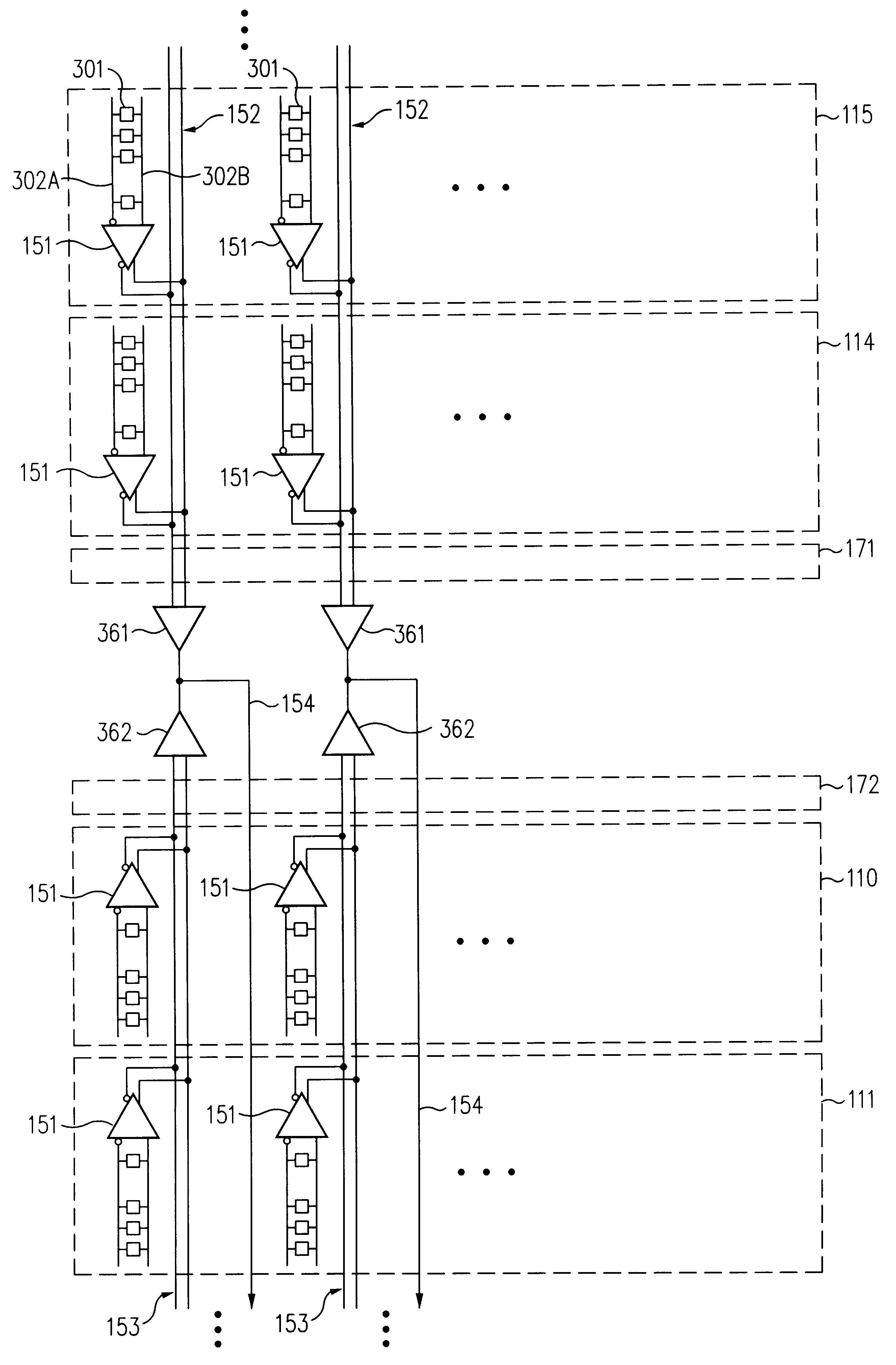
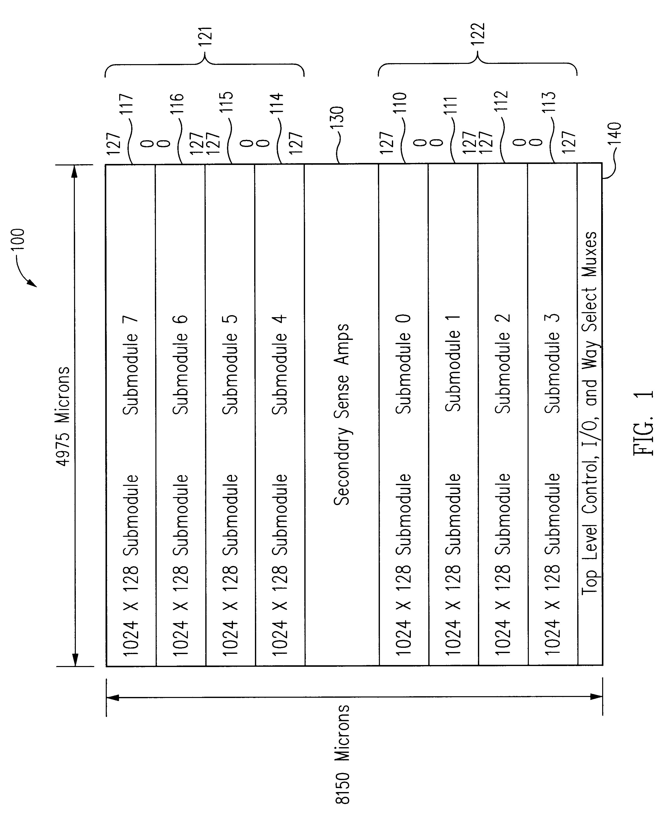
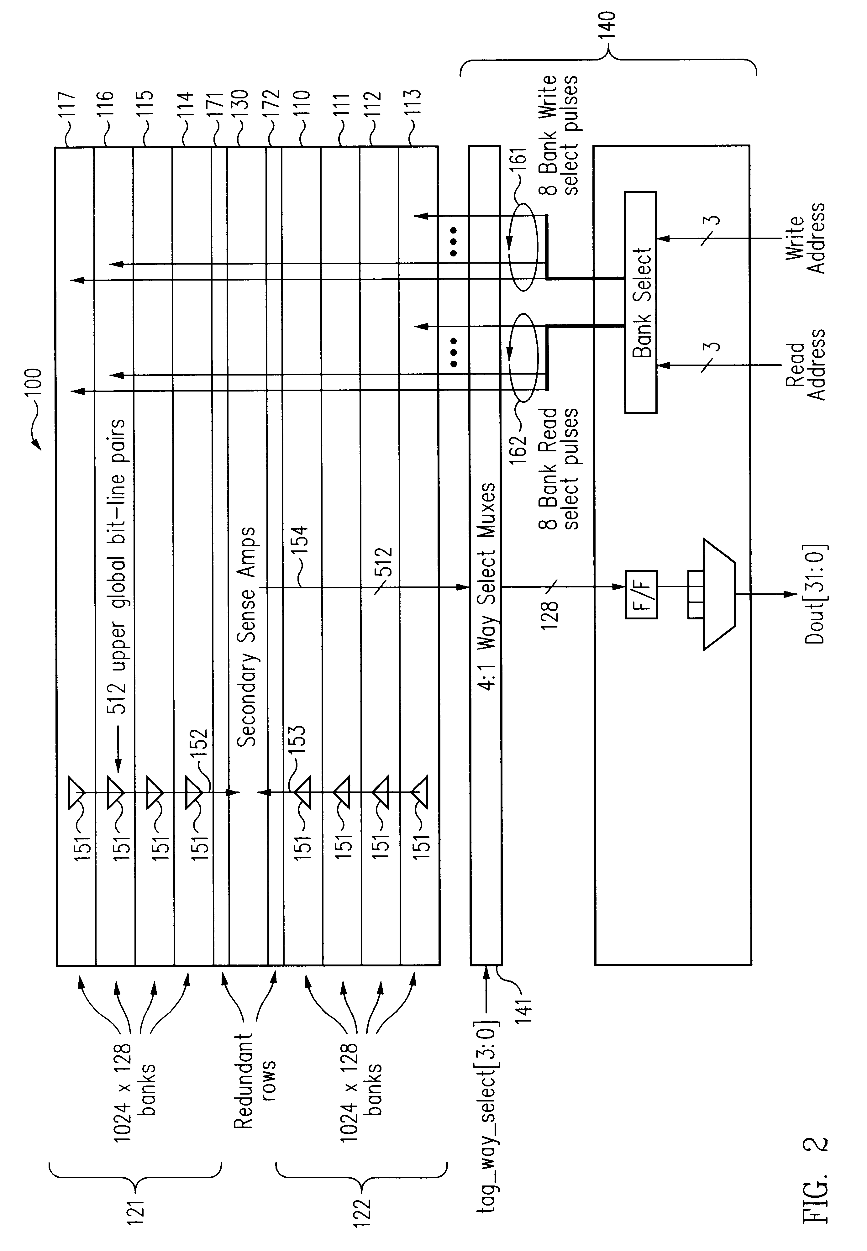
FIG. 1 depicts the organization and layout of a memory module 100 in accordance with an exemplary embodiment of the present invention. Eight submodules or banks 110, 111, 112, 113, 114, 115, 116 and 117 are organized into upper and lower groups 121 and 122. In the embodiment of FIG. 1, the submodules are substantially identical and each includes an array of memory cells, word line drivers and word line decoders, column decoders, primary sense amplifiers, write drivers, equilibrate circuits, and control circuitry (not shown). In this regard, the submodules are conventional and, based on the description herein, a variety of suitable configurations will be appreciated by persons of ordinary skill in the art. However, in accordance with some embodiments of the present invention, advantageous primary sense amplifier configurations are described in greater detail below with reference to FIG. 4. Secondary sense amplifiers 130 (FIG. 1) are positioned toward the center of memory module 100 b...


PUM


Abstract

A memory module configuration has been developed, which employs multi-level sensing, low-voltage-swing differential signal paths, and array layout techniques to better optimize area / speed / power tradeoffs. In some configurations two-level sensing is employed with secondary sense amplifiers positioned toward a middle of the memory module with memory banks or submodules positioned therearound. Primary sense-amplifiers in the submodules or banks sense differential signals on local bit-lines spanning the corresponding submodule or bank and drive a low-voltage-swing differential signal onto global bit-lines that span a subset of the submodules or banks. The global bit-lines are sensed by secondary sense amplifiers that drive data outputs across a subset of the submodules or banks toward output circuits. In some configurations the memory module is divided into upper and lower portions with upper global bit-lines spanning the upper portion and lower global bit-lines spanning the lower portion. Corresponding upper and lower global bit-lines are disjoint and are sensed by corresponding upper and lower secondary sense amplifiers. By this arrangement, the minimum to maximum variation in access time between the different rows of the memory module is reduced. Moreover, smaller drivers and lower power is achieved by use of such a two-level arrangement. In particular, area reductions and power reductions are achieved for submodule- or bank-resident primary sense amplifiers.

Description

1. Field of the InventionThe present invention relates to semiconductor memories, and in particular, to organization and layout thereof.2. Description of the Related ArtSemiconductor memories are characterized by regular repetition of memory cells, which are typically organized in an hierarchical addressing topology. Each memory cell is associated with a unique address that typically identifies a particular row and column in a matrix. A group of memory cells is selected by activating a row line (or in some configurations, a word line) to which cells of the group are connected. This enables each of the memory cells so selected, when in a read access mode, to drive its associated column line (or in some configurations, bit-line) in a manner corresponding to the data stored therein. Alternatively, when in a write access mode, each of the selected memory cells is enabled to receive data conveyed on the bit-line to the memory cell.There are many ways to arrange a bit-line configuration a...

Claims


Application Information

Patent Timeline
13 Feb 2001
Publication
US6188596B1
IPC
G11C5/02; G11C7/18; G11C7/00
CPC
G11C5/025; G11C7/18
Inventors
HOLST, JOHN CHRISTIAN