Insulated gate semiconductor device and method of manufacturing the same

a technology of insulated gate and semiconductor device, which is applied in the direction of semiconductor devices, electrical appliances, nanotechnology, etc., can solve the problems of difficult control of current flowing in the channel region, deterioration of sub-threshold characteristics, and difficulty in fine machining in the order of sub-microns

Inactive Publication Date: 2001-03-06
SEMICON ENERGY LAB CO LTD
View PDF33 Cites 95 Cited by
  • Summary
  • Abstract
  • Description
  • Claims
  • Application Information

AI Technical Summary

Problems solved by technology

However, the fine machining in the order of the sub-micron suffers from a problem that it does not simply accord to the scaling rule.
In other words, an on-state current is changed according to a complicated electric field distribution, thereby making it difficult to control the current which flows in the channel region 303 by only the gate voltage Vg.
Also, there has been known that a sub-threshold characteristic is deteriorated when an influence of the gate voltage on the drain current by the punch-through phenomenon is lowered.
The deterioration of the threshold value voltage is desirable from a viewpoint of lowering a power consumption, however, there generally arises such a disadvantage that a frequency characteristic is not increased because the drive voltage of th

Method used


Image

  • Insulated gate semiconductor device and method of manufacturing the same
  • Insulated gate semiconductor device and method of manufacturing the same
  • Insulated gate semiconductor device and method of manufacturing the same

Examples


embodiment 1

(Embodiment 1)

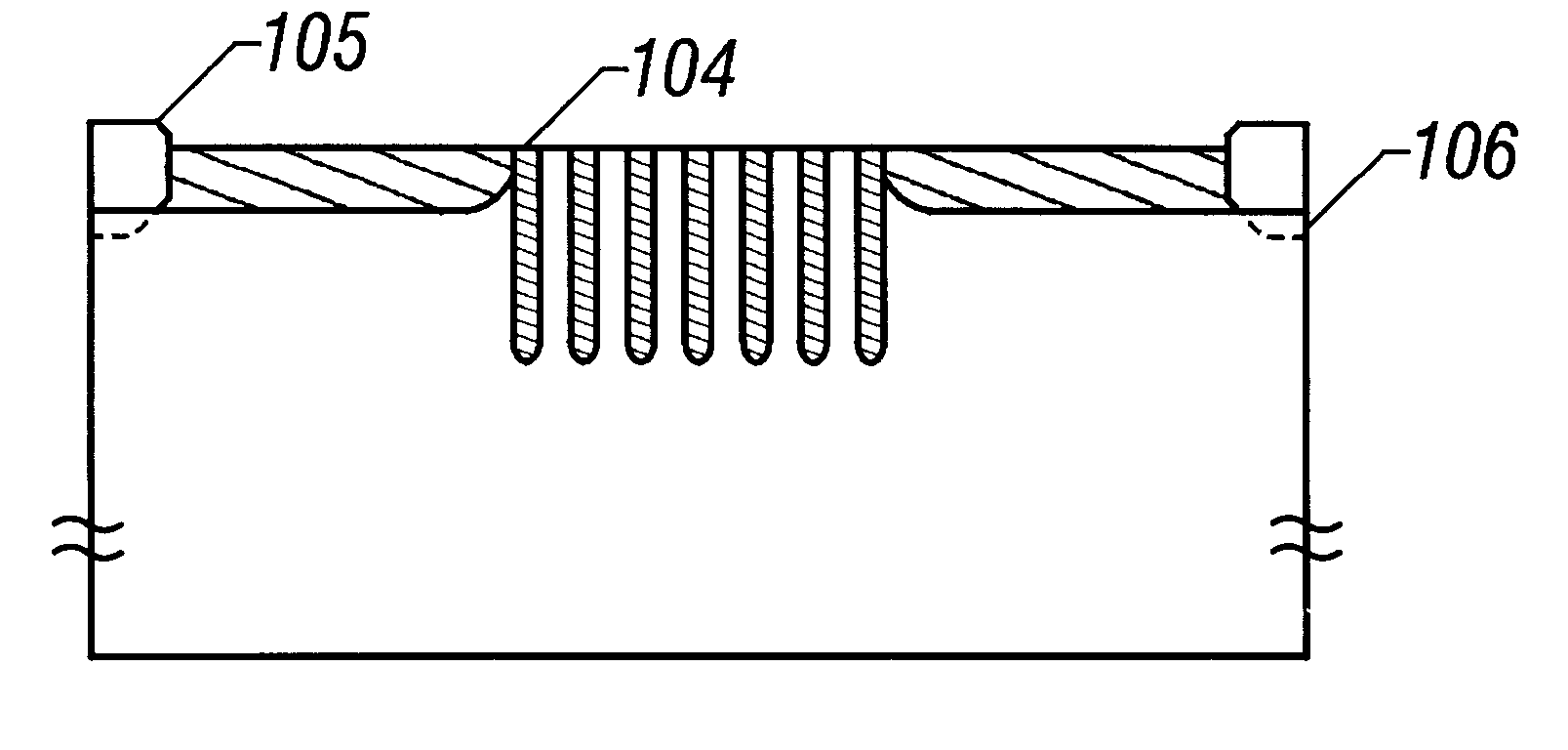
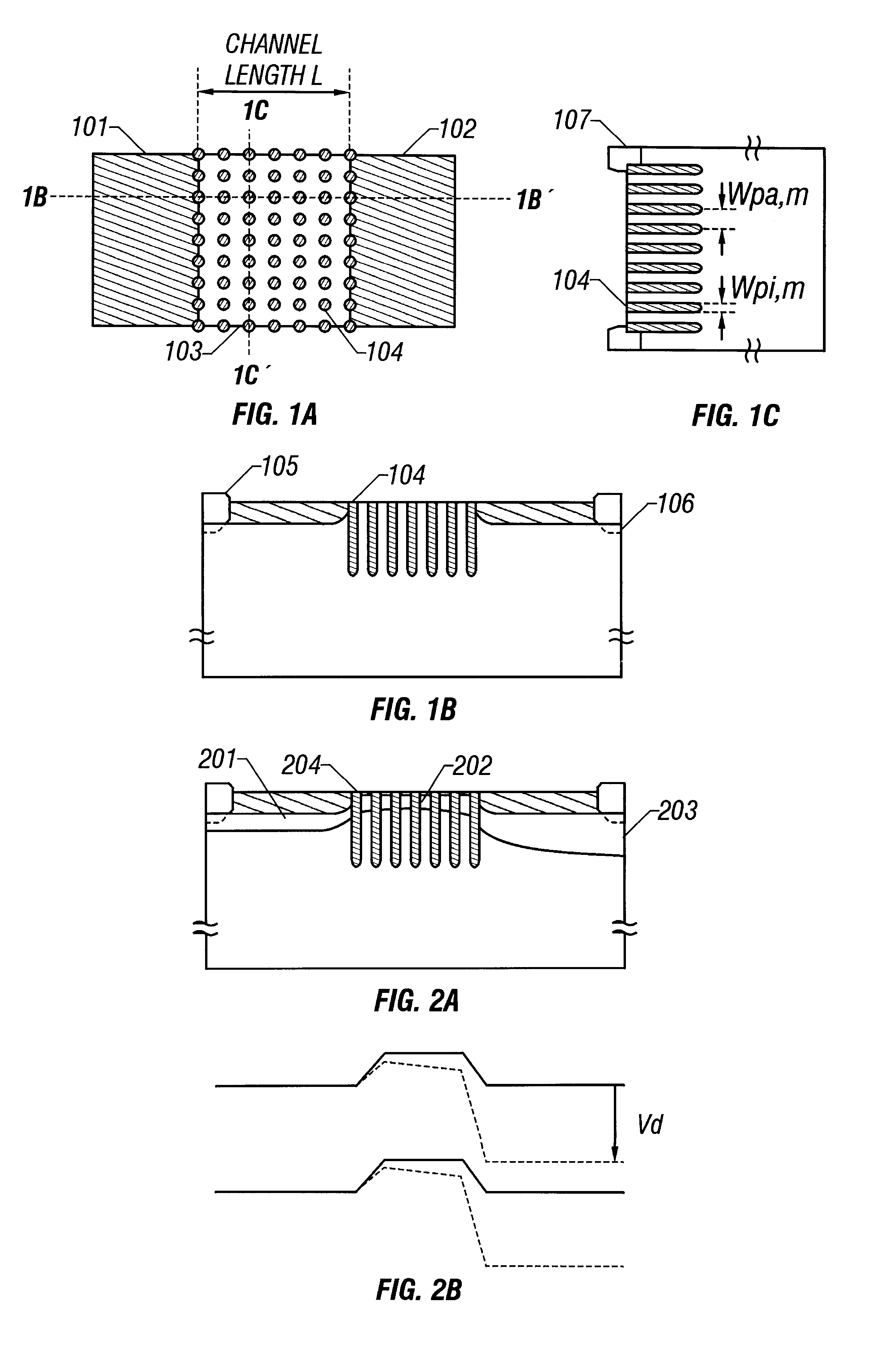
An example in which an insulated gate electric field effect transistor is formed on a monocrystal silicon substrate in accordance with the present invention will be described with reference to FIGS. 7A to 7E. In this embodiment, for simplification of description, there is shown an example in which a single n-channel FET is formed on a p-type silicon substrate.

First, reference numeral 701 denotes a p-type silicon substrate on which a silicon oxide film 702 is formed as a pad oxide film on which a silicon nitride film 703 that functions as a mask which will be used later for selective oxidation is further formed. The thickness of the silicon oxide film 702 and the silicon nitride film 703 may be 500 to 2000 .ANG. (FIG. 7A).

Then, patterning is conducted so that the silicon nitride film 703 remains only in the device formation region, and in this state, ions of impurity elements that give p-type conduction are implanted into the silicon nitride film 703. Thereafter, wet ox...

embodiment 2

(Embodiment 2)

In this embodiment, there is shown an example of structuring a CMOS circuit with a complementary combination of an n-channel FET (NMOS) and a p-channel FET (PMOS) in accordance with the present invention. Although the details of a process of manufacturing the CMOS circuit will-be omitted here, the impurity regions shaped in a dot pattern is formed only in the channel forming region before forming the gate insulating film according to the present invention, as was described in the embodiment 1.

FIG. 13A shows a cross-sectional view of a CMOS circuit in accordance with the present invention. FIG. 13A is a cross-sectional view of the CMOS circuit cut along the channel direction, which is formed through a normal manufacturing method.

In FIG. 13A, reference numeral 1301 denotes an n-type silicon substrate, reference numeral 1302 denotes a n-well, and-reference numeral 1303 denotes a p-well. In other words, a p-channel FET (PMOS) is formed on the n-well 1302, and an n-channel ...

embodiment 3

(Embodiment 3)

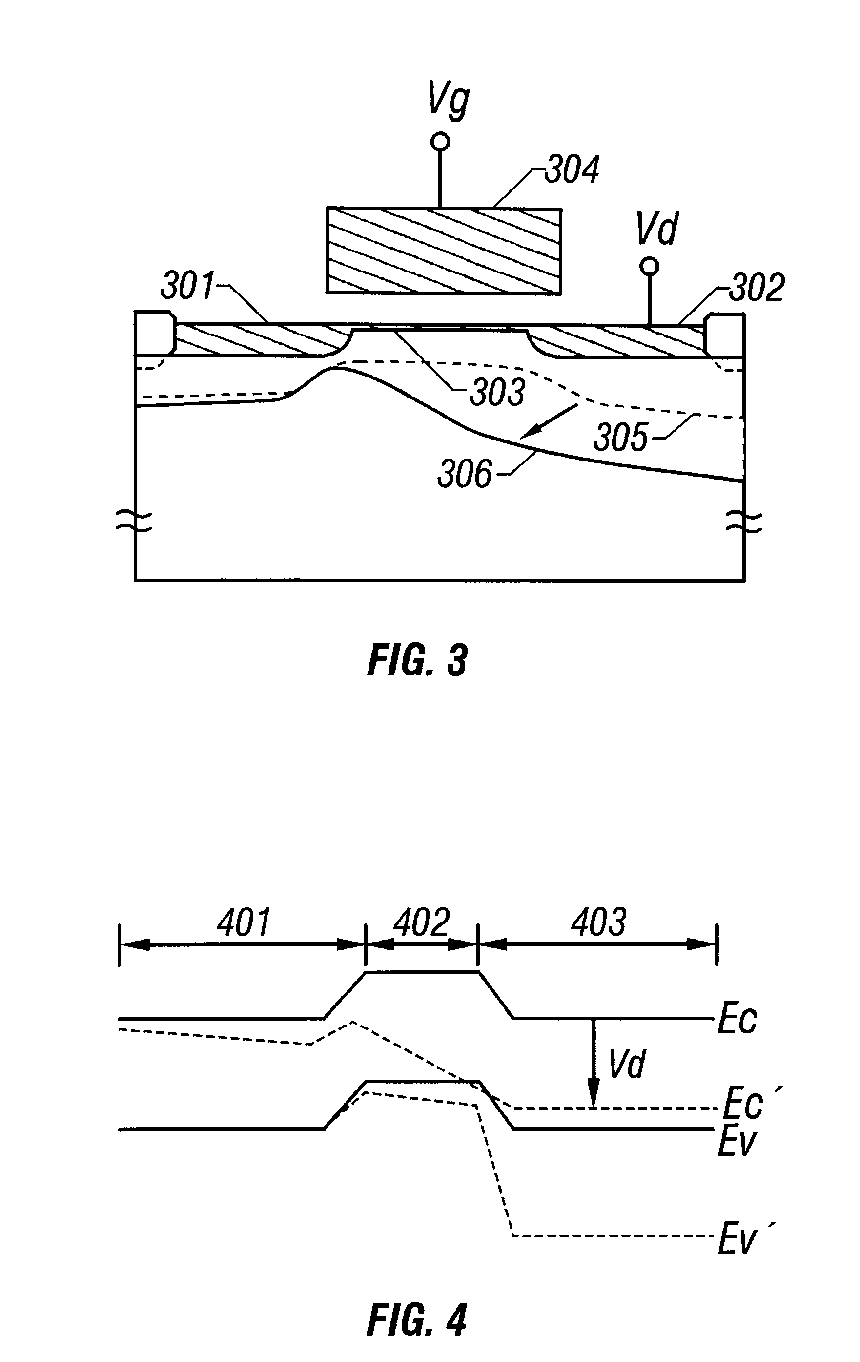
In the embodiment 1, a depthwise shape of the impurity region 707 is shaped in a bar. However, this is a shape under an ideal state where no scattering occurs when implanting ions. In fact, the impurity regions which are variously shaped can be formed depending on conditions when implanting ions.

For example, an impurity region 901 which is shaped in wedges as shown in FIG. 9A can be formed depending on the conditions where ions are implanted. Also, reversely, an impurity region 902 which is shaped in droplets as shown in FIG. 9B may be formed. In particular, in case of the shape shown in FIG. 9B, the impurity regions adjacent to each other on a lower portion of the impurity region 902 are in contact with each other.

In this state, it can be substantially regarded as an SOI structure where the channel forming region is insulatingly separated from a bulk substrate. This structure can extremely effectively restrain the drain side depletion layer from influencing the deplet...


PUM


Abstract

Dot-pattern-like impurity regions are artificially and locally formed in a channel forming region. The impurity regions restrain the expansion of a drain side depletion layer toward the channel forming region to prevent the short channel effect. The impurity regions allow a channel width W to be substantially fined, and the resultant narrow channel effect releases the lowering of a threshold value voltage which is caused by the short channel effect.

Description

1. Field of the InventionThe present invention relates to the structure of an insulated gate semiconductor device formed using a crystalline semiconductor substrate, for example, a monocrystal silicon substrate or an SOI substrate (SIMOX or the like), and more particularly to the structure of an insulated gate field effect transistor (hereinafter referred to simply as "IG-FET") and a method of manufacturing the same. The present invention relates to a technique of which advantages are especially exhibited in the case of manufacturing a fine device whose channel length is 1 .mu.m or less (representatively, 0.01 to 0.35 .mu.m.Therefore, the present invention is applicable to a semiconductor integrated circuit such as an IC, a VLSI or a ULSI, which is structured with integrated IG-FETs.2. Description of the Related ArtIn recent years, integrated circuits such as the VLSI are kept on becoming more fine, and the machining dimensions in the order of a deep sub-micron are required, for exa...

Claims


Application Information

Patent Timeline
IPC IPC(8): H01L29/167H01L21/70H01L29/06H01L29/66H01L21/8238H01L29/10H01L21/8249H01L29/786H01L29/15H01L27/092H01L27/085H01L27/06H01L29/165H01L29/02H01L29/78H01L27/12
CPCB82Y10/00H01L21/823807H01L21/8249H01L27/0623H01L27/092H01L29/0615H01L29/0619H01L29/0649H01L29/1033H01L29/158H01L29/165H01L29/167H01L29/78696H01L27/12
Inventor YAMAZAKI, SHUNPEIOHTANI, HISASHIFUKUNAGA, TAKESHI
Owner SEMICON ENERGY LAB CO LTD
Why Eureka
Try Eureka