Electromigration resistant power distribution network

a technology of power distribution network and electromigration resistance, applied in the direction of instruments, computer aided design, basic electric elements, etc., can solve the problems of not recognizing, teaching or suggesting the benefits of increased electromigration resistance and greater grid redundancy

Inactive Publication Date: 2001-03-13
IBM CORP
View PDF3 Cites 85 Cited by
  • Summary
  • Abstract
  • Description
  • Claims
  • Application Information

AI Technical Summary

Problems solved by technology

U.S. Pat. No. 5,742,099 thus teaches the segmentation of the power and ground busses to improve wireability of control logic using automat...

Method used


Image

  • Electromigration resistant power distribution network
  • Electromigration resistant power distribution network
  • Electromigration resistant power distribution network

Examples


Embodiment Construction

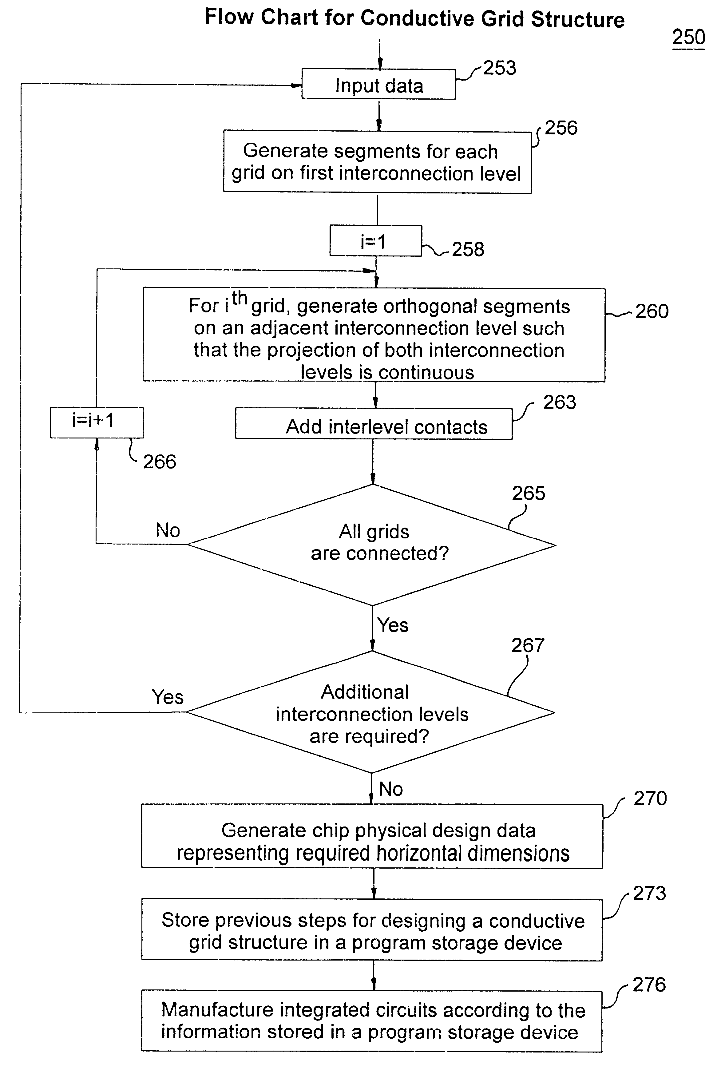
The present invention is a method and apparatus for increasing the electromigration resistance of an IC power distribution grid while still maintaining the redundancy and low resistance of the power grid.

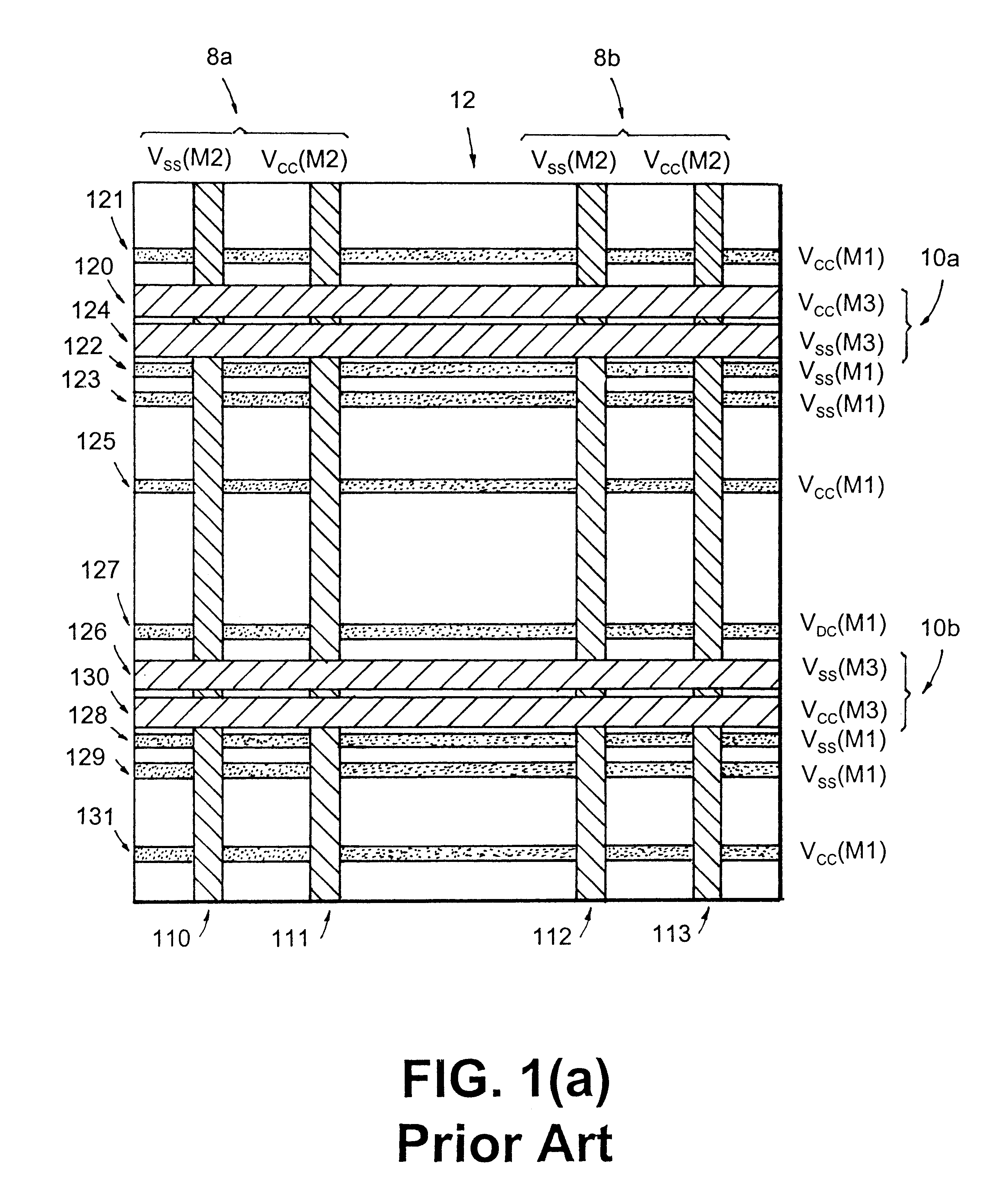
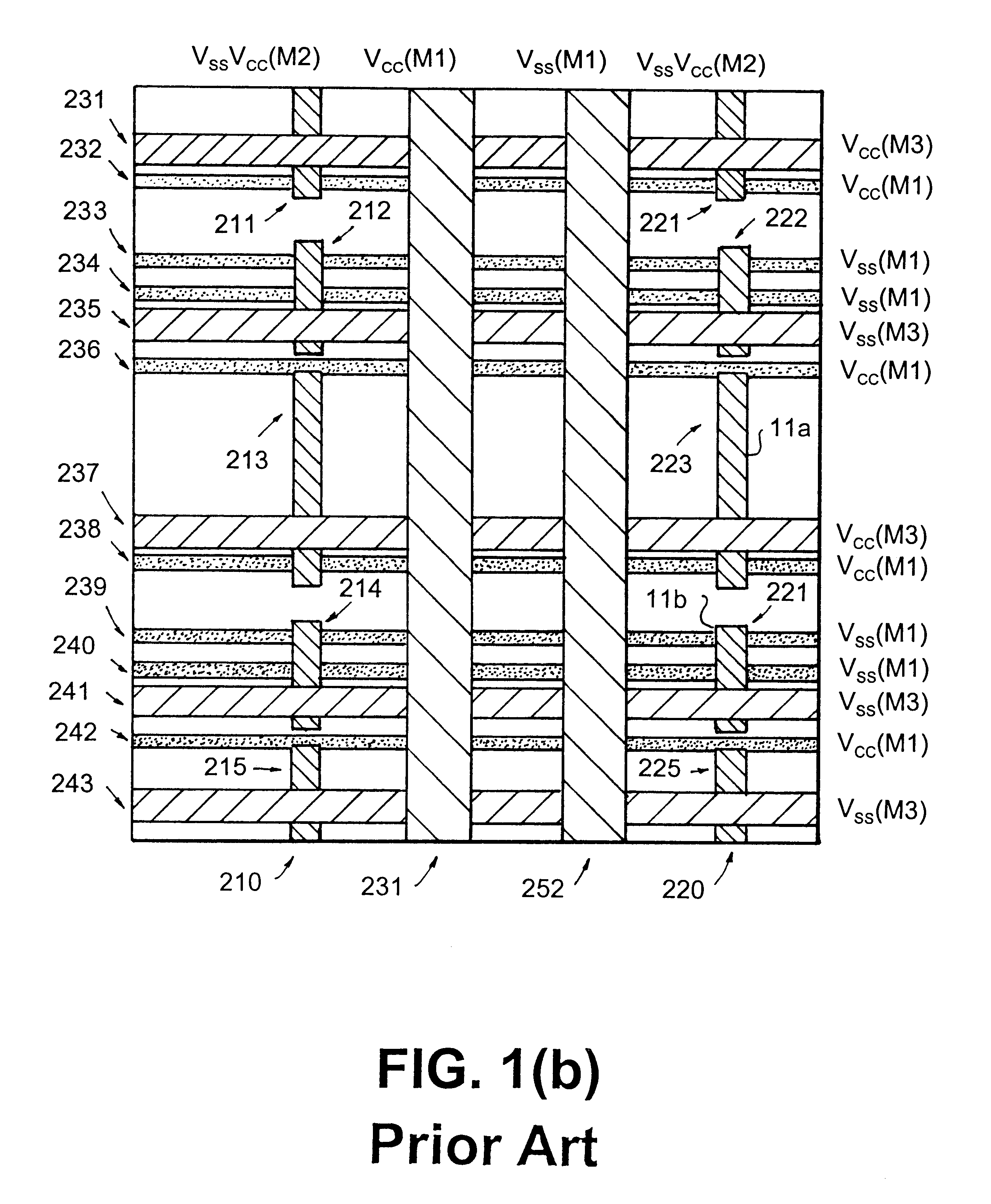
FIG. 2(d) illustrates the power distribution grid pattern 400 according to the invention. As shown in FIG. 2(d), the grid pattern 400 has a similar geometry as orthogonal grid of lines according to the prior art, however, is made up entirely of line segments that are only about four times larger than the dimension of the cell size of the grid and further includes gaps, e.g., gaps 55a in a vertical dimension and gaps 55c in a horizontal dimension that are "phase shifted" with respect to gaps, e.g., gaps 55b, 55d, respectively, of adjacent tracks (in the same dimension) of the segmented power line. In current designs, the cell size is about 25 microns. Thus, line segments of 100 micro meters may be used to layout the grid which length has been determined to exhibit significantly bette...


PUM


Abstract

Method for forming a novel power grid structure for integrated circuit semiconductor chip devices that exhibits increased electromigration resistance by including diffusion blocking interlevel contacts and employing a regular array of conducting line elements with "phase shift" between adjacent tracks of segmented power busses. The novel grid structure includes a first metal layer including a first set of conducting line segments that are substantially parallel to one another and run in a first direction; a layer of diffusion blocking dielectric insulation above the first layer; a second metal layer including a second set of conducting line segments substantially parallel to each other and running in a second direction orthogonal to the first direction; and, interlevel contact studs disposed substantially vertically through the diffusion blocking dielectric insulation layer for electrically connecting aligned line segments of the first and second sets, wherein each segment of the first and second sets of line segments is limited to a predetermined length by a diffusion blocking boundary.

Description

1. Field of the InventionThe present invention relates to power distribution schemes in integrated circuit chips (ICs), and specifically, to a novel power distribution network for ICs that exhibits increased electromigration resistance while maintaining redundancy and lower resistance.2. Discussion of the Prior ArtPower for integrated circuits is usually distributed on a chip by a grid of continuous metal lines. Typically, there are two separate grids; one at ground potential and one at Vdd.As illustrated in FIG. 1(a), a "continuous" grid 12 may be formed from orthogonal sets of lines on respective two different wiring levels in the chip. Specifically, a set of parallel lines 8a, 8b for example, is patterned at one chip wiring level and are connected to a second orthogonal set of lines 10a, 10b on the second wiring level via studs so as to form the continuous grid. In present chip designs, the length of the lines is determined by the size of the area over which power must be distrib...

Claims


Application Information

Patent Timeline
IPC IPC(8): G06F17/50H01L21/70H01L21/768H01L23/528H01L23/52H01L23/532
CPCG06F17/5077H01L21/76841H01L21/7685H01L21/76858H01L23/5286H01L23/53223H01L2924/0002H01L2924/00G06F30/394
Inventor FILIPPI, RONALD G.LIN, PHILLIP C.SHAW, THOMAS M.WACHNIK, RICHARD A.
Owner IBM CORP
Why Eureka
Try Eureka