Cobalt salicidation method on a silicon germanium film

a technology of cobalt and germanium, applied in the field of cobalt salicidation can solve the problems of source/drain contact resistance negatively affecting device performance, the structure and method of conventional mos transistor fabrication cannot be simply "scaled down" to produce smaller transistors for higher density integration, and the technique is unable to form a low-resistance cobalt silicide film on silicon germanium alloy

Inactive Publication Date: 2001-04-10
INTEL CORP
View PDF3 Cites 227 Cited by
  • Summary
  • Abstract
  • Description
  • Claims
  • Application Information

AI Technical Summary

Problems solved by technology

Unfortunately, the structure and method of fabrication of conventional MOS transistors cannot be simply "scaled down" to produce smaller transistors for higher density integration.
As device features are continual...

Method used


Image

  • Cobalt salicidation method on a silicon germanium film
  • Cobalt salicidation method on a silicon germanium film
  • Cobalt salicidation method on a silicon germanium film

Examples


Embodiment Construction

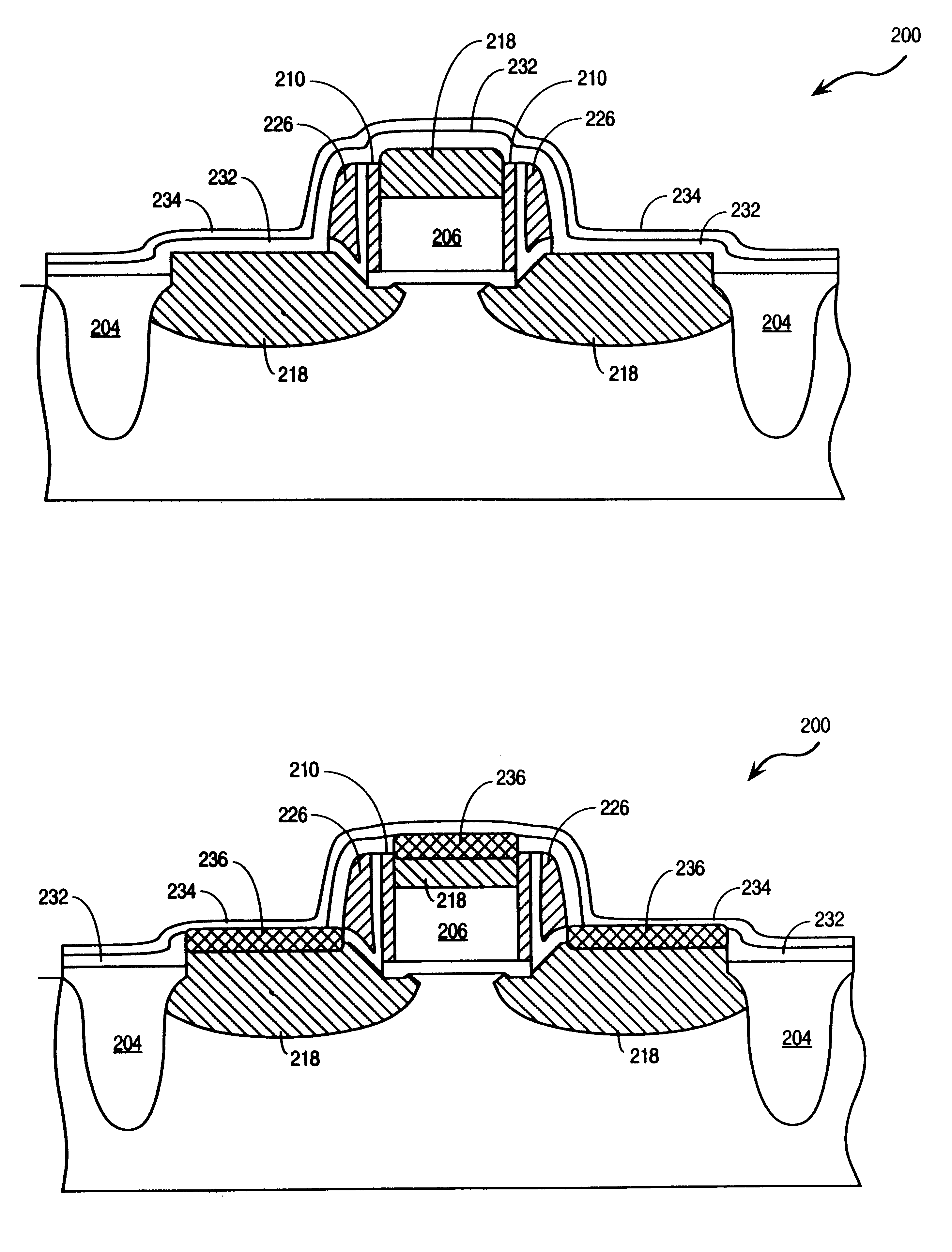
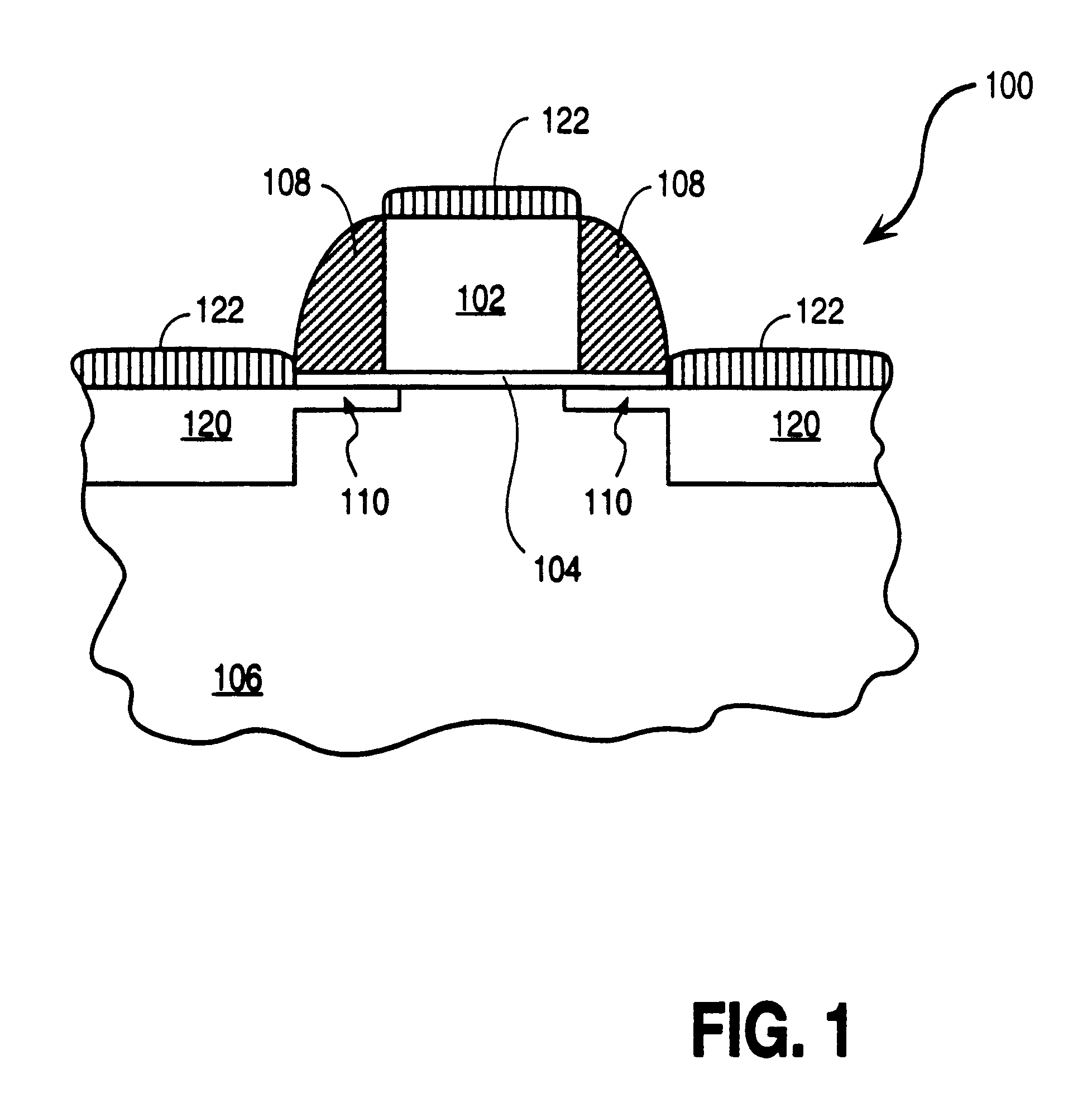
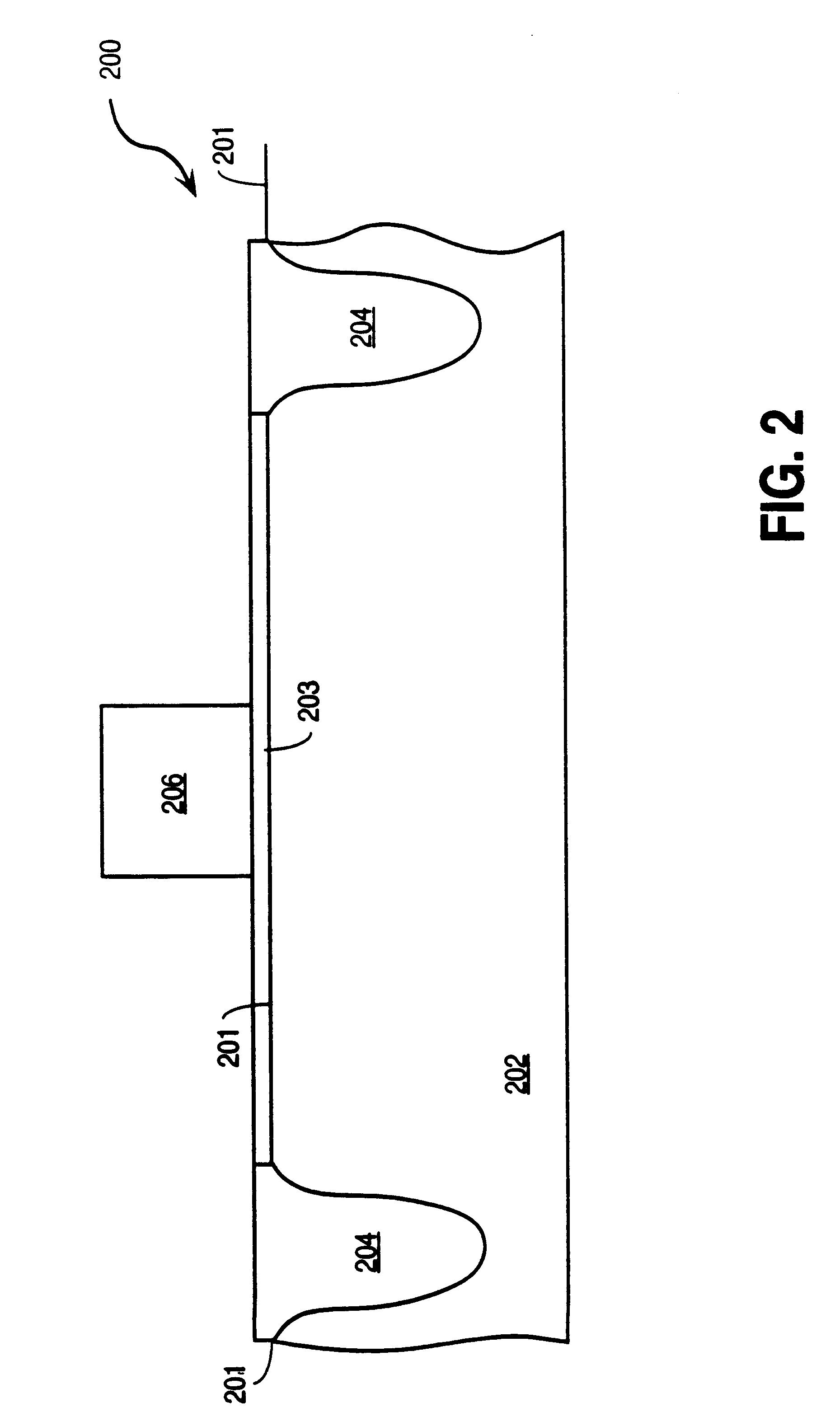
A novel method for forming a cobalt silicide film on a silicon germanium alloy is described. In the following description numerous specific details are set forth such as specific materials, dimensions, and processes etc. in order to provide the through understanding in the present invention. It will be obvious, however, to one skilled in the art that the present invention may be practiced without the specific details. In other instances well known semiconductor equipment and processes have not been described in particular detail in order to avoid unnecessarily obscuring the present invention.

The present invention is a novel cobalt (Co) salicidation process carried out on a silicon germanium alloy. According to the present invention a cobalt film is deposited on to a silicon germanium alloy formed on a substrate. The substrate is then heated to a temperature greater than 850.degree. C. an ideally to greater 900.degree. C. for a period of time of less than 20 seconds and ideally less ...


PUM


Abstract

A method of forming a cobalt germanosilicide film is described. According to the present invention a silicon germanium alloy is formed on a substrate. A cobalt film is then formed on the silicon germanium alloy. The substrate is then heated to a temperature of greater than 850° C. for a period of time less than 20 seconds to form a cobalt germanium silicide film.

Description

1. Field of the InventionThe present invention relates to the field of semiconductor manufacturing and more specifically to a cobalt silicide film on a silicon germanium alloy.2. Discussion of Related ArtToday literally millions of individual transistors are coupled together to form very large-scale integrated (VSLI) circuits, such as microprocessors, memories, and application specific integrated circuits (IC's). Presently, the most advanced IC's are made up of approximately three million transistors, such as metal oxide semiconductor (MOS) field effect transistors having gate lengths on the order of 0.25 .mu.m. In order to continue to increase the complexity and computational power of future integrated circuits, more transistors must be packed into a single IC (i.e., transistor density must increase). Thus, future ultra large-scale integrated (ULSI) circuits will require very short channel transistors with effective gate lengths less than 0.1 .mu.m. Unfortunately, the structure and...

Claims


Application Information

Patent Timeline
IPC IPC(8): H01L21/336H01L21/02H01L21/28H01L29/49H01L21/285H01L29/45H01L29/40H01L29/04H01L29/165H01L29/02
CPCH01L29/41783H01L29/456H01L29/4941H01L29/665H01L29/66636H01L21/28052H01L21/28518H01L21/28525H01L21/28562H01L29/045H01L29/165
Inventor MURTHY, ANANDCHAU, ROBERT S.
Owner INTEL CORP
Why Eureka
Try Eureka