Thermoelectric semiconductor compound and method of making the same

Inactive Publication Date: 2001-05-01
AISIN SEIKI KK
View PDF5 Cites 52 Cited by
  • Summary
  • Abstract
  • Description
  • Claims
  • Application Information

AI Technical Summary

Problems solved by technology

As long as improvements in the performance index Z require a trade-off

Method used


Image

  • Thermoelectric semiconductor compound and method of making the same
  • Thermoelectric semiconductor compound and method of making the same
  • Thermoelectric semiconductor compound and method of making the same

Examples


Embodiment Construction

Preferred embodiments of the present invention will be described hereinafter in detail with reference to the accompanying drawings.

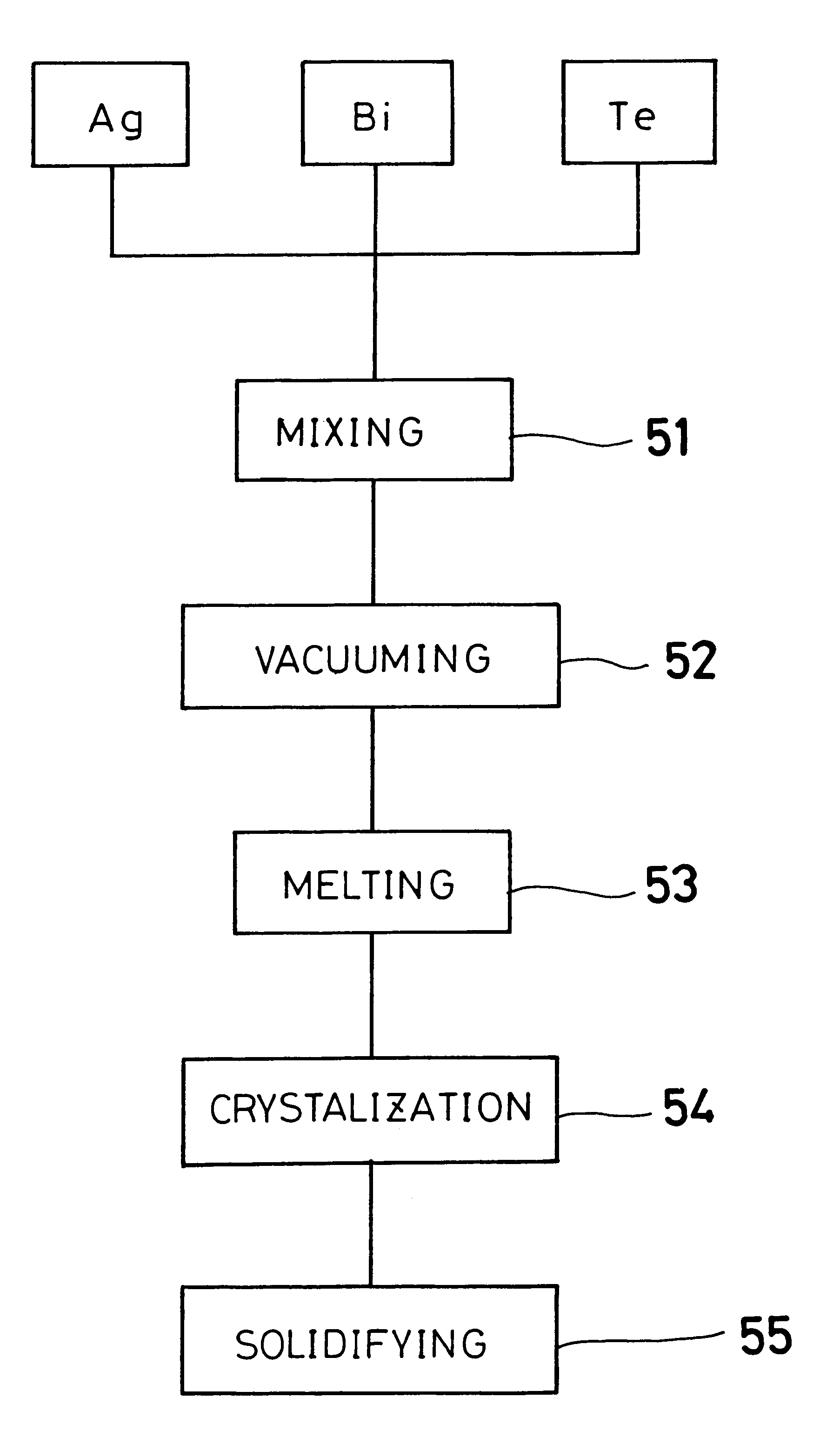
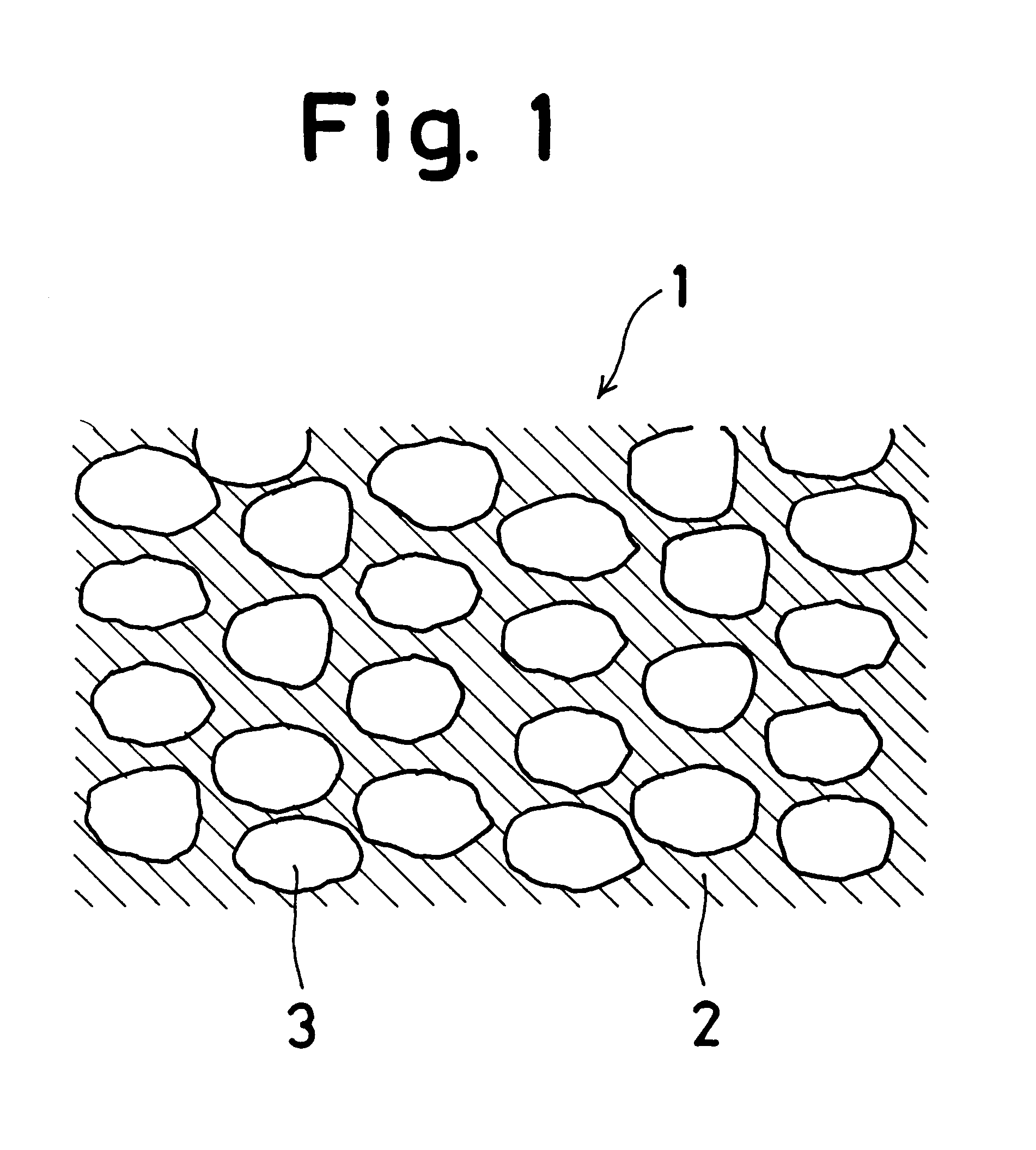
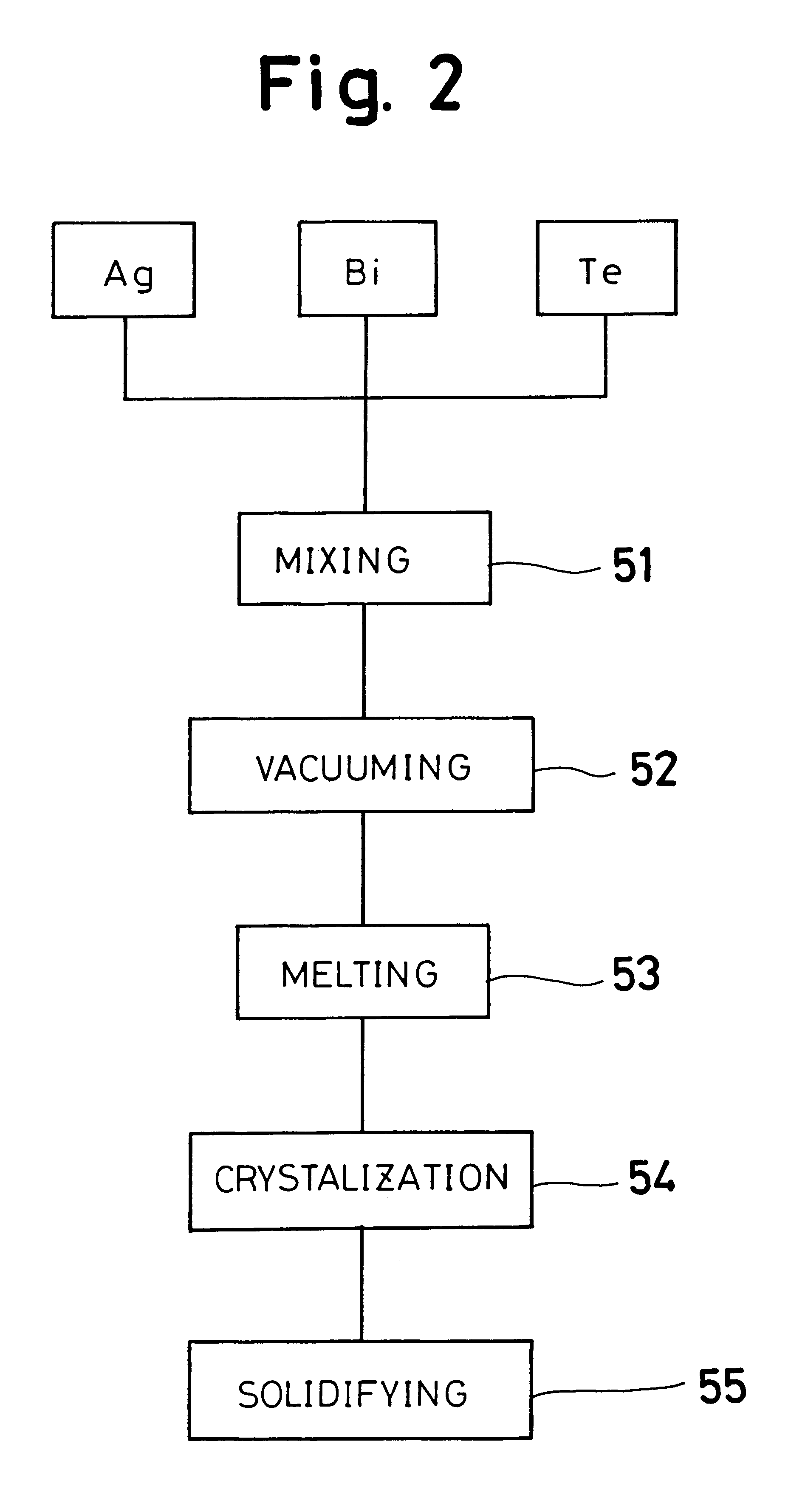
In accordance with a first embodiment of the present invention, FIG. 1 shows a thermoelectric semiconductor compound 3 including a first thermoelectric semiconductor 1, which is in the form of a matrix, and a second thermoelectric semiconductor 2, which is in the form of particles dispersed in the matrix. The first thermoelectric semiconductor 1 and the second thermoelectric semiconductor 2 have a common element, and an average diameter D of the dispersed particles complies with a formula of A

For example, the first semiconductor 1 can be a member of the BiTe.sub.3 family of semiconductors. In particular, the first thermoe...


PUM


Abstract

A thermoelectric semiconductor compound is provided whose performance index Z is remarkably improved without sacrificing Seebeck coefficient, electrical conductivity or thermal conductivity. The thermoelectric semiconductor compound includes a first thermoelectric semiconductor which is in the form of matrix and a second thermoelectric semiconductor which is in the form of particles dispersed in the matrix. The first thermoelectric semiconductor and the second thermoelectric semiconductor have a common element. The average diameter D of the dispersed particles complies with a formula of A<D<B, where A is the mean free path of a carrier in a single crystal of the second thermoelectric semiconductor and B is the mean free path of a long wave length phonon in the single crystal of the second thermoelectric semiconductor. A method for making the a thermoelectric semiconductor compound is provided.

Description

1. Field of the InventionThe present invention is directed to a thermoelectric semiconductor compound and a method of making the thermoelectric semiconductor compound.2. Description of Related ArtIt is well known that thermoelectric semiconductor compounds exhibit the Seebeck effect, where heat is converted to electricity, and the Peltier effect, where application of an electric current causes cooling or heating.The thermoelectric performance of a thermelectric semiconductor compound is indicated by a performance index Z (=.alpha..sup.2.sigma. / .kappa., where .alpha. is the Seebeck coefficient, .sigma. is the electrical conductivity, and .kappa. is the thermal conductivity). A higher performance index Z results in higher thermoelectric performance. For example, a higher performance index Z results in a higher voltage being developed if a temperature difference is provided across a thermoelectric semiconductor. A higher performance index Z also results in a larger temperature differen...

Claims


Application Information

Patent Timeline
IPC IPC(8): H01L35/12H01L35/16H01L35/26H01L35/34
CPCH01L35/16H10N10/852
Inventor SAKAKIBARA, TSUTOMUIMOTO, TAKANORITAKIGAWA, YASUO
Owner AISIN SEIKI KK
Why Eureka
Try Eureka