

Flip chip package for micromachined semiconductors
- Summary
- Abstract
- Description
- Claims
- Application Information
AI Technical Summary
Problems solved by technology
Method used
Image

Examples
Embodiment Construction
(S)
1. Field of the Preferred Embodiment(s)
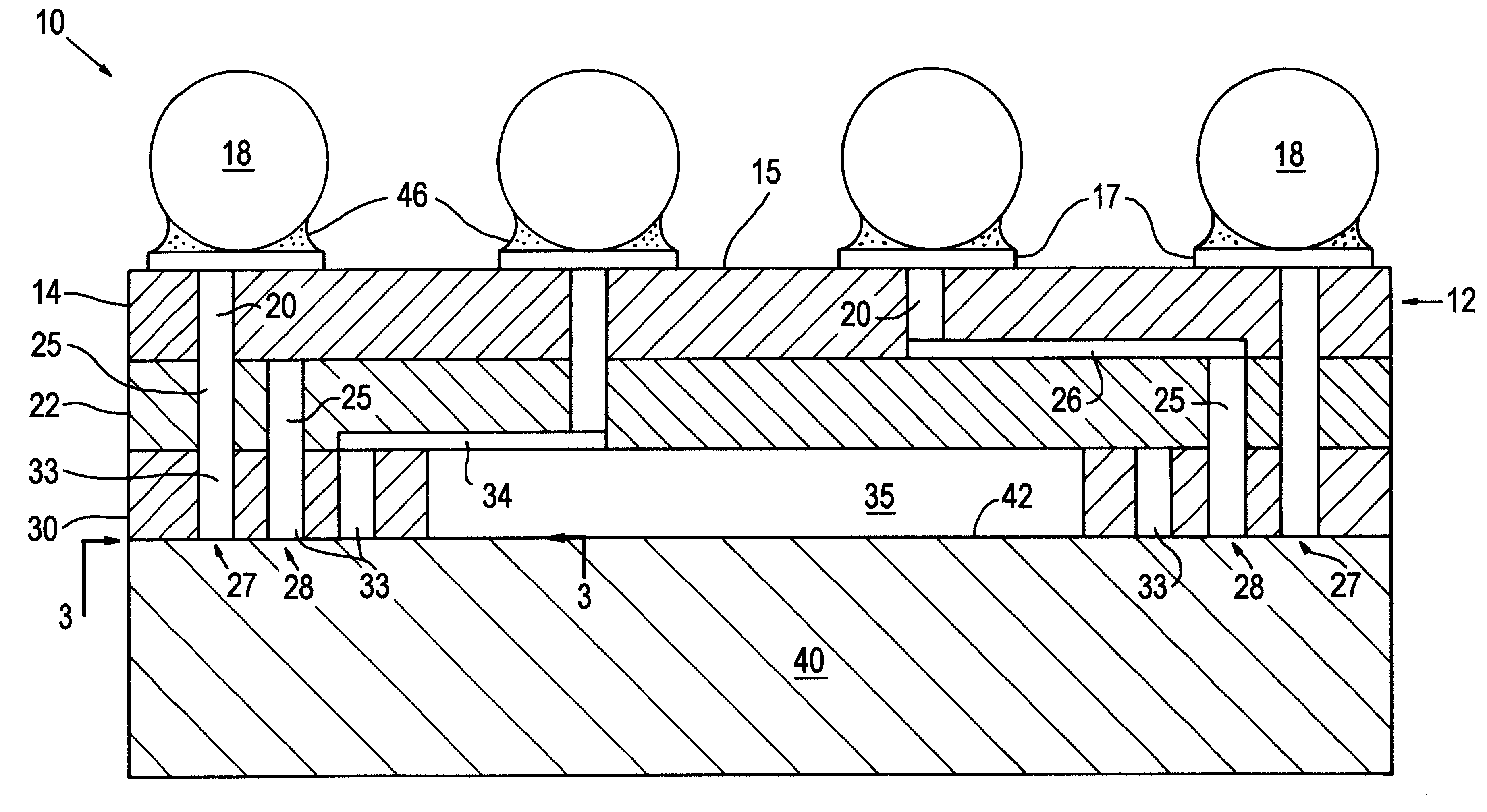
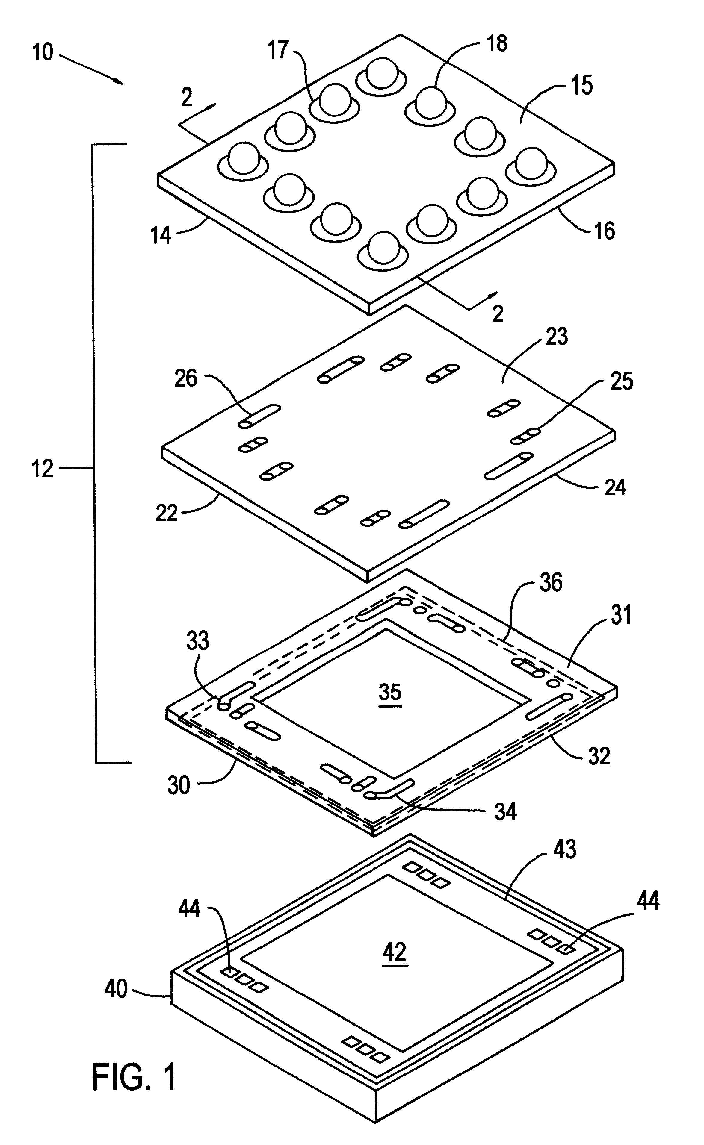
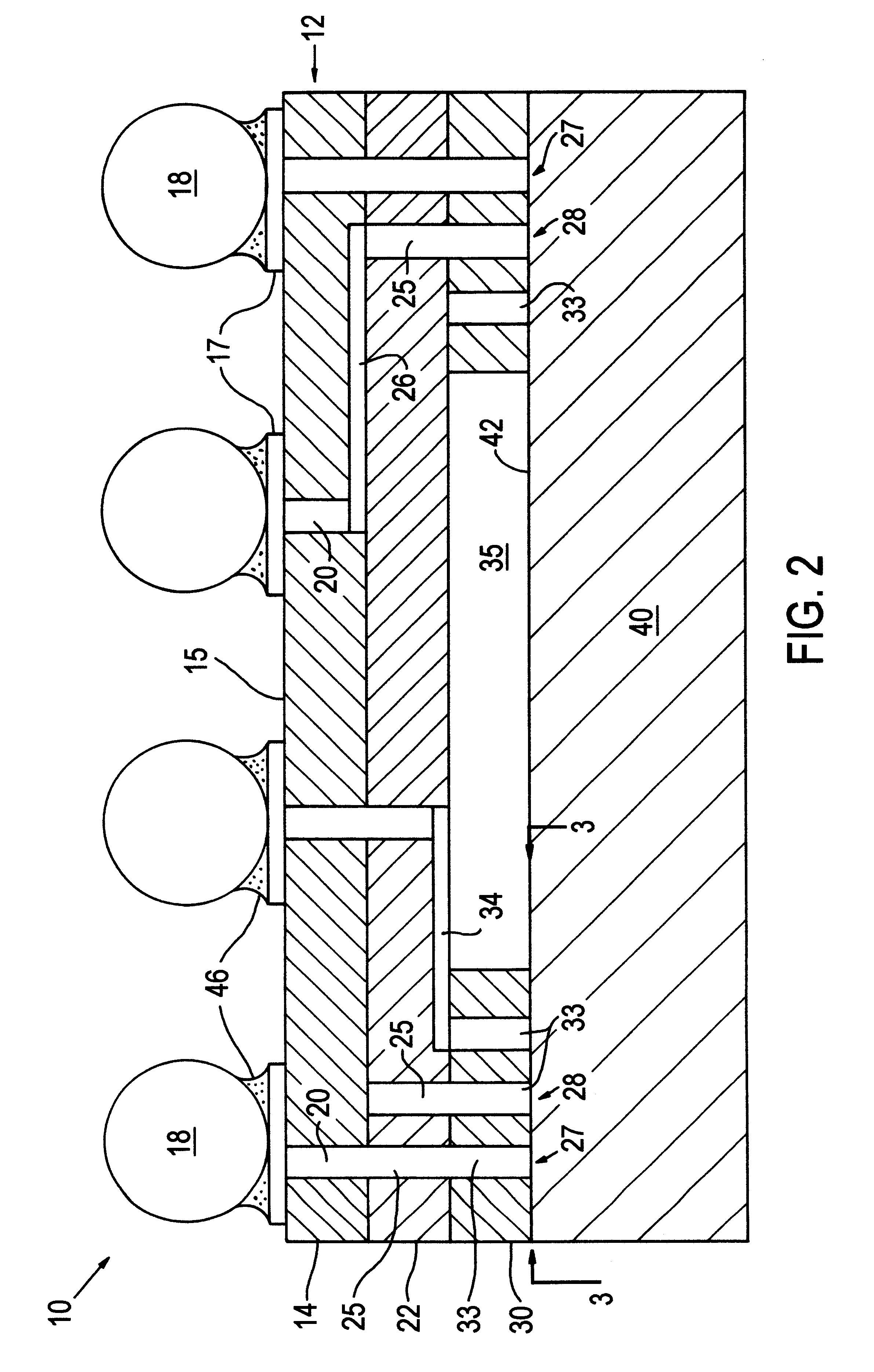
This invention generally relates to ceramic electronic packaging. Specifically, there is a multilayered ceramic package having a cavity that is bonded to a micromachined semiconductor device.
2. Description of the Related Art
Various devices and techniques are used for packaging of micromachined semiconductor devices. Typically, a micromachined semiconductor die is fabricated with wirebond pads and a sealing structure. A silicon lid has a cavity etched therein using a strong acid such as hydrofluoric. The micromachined semiconductor needs space within the package to allow the moving surfaces of the device to function properly. The silicon lid can be attached to the semiconductor die by an adhesive. The die and lid assembly is placed on a hybrid ceramic where the bond pads on the die are wirebonded to bond pads on the hybrid ceramic. The hybrid ceramic is then encapsulated within a hermetic package. This package has several problems. First, wir...
PUM
| Property | Measurement | Unit |
|---|---|---|
| electrical | aaaaa | aaaaa |
| temperature | aaaaa | aaaaa |
| semiconductor | aaaaa | aaaaa |
Abstract
Description
Claims
Application Information