Method of manufacturing crystal of silicon using an electric potential

a technology of electric potential and crystal, which is applied in the direction of crystal growth process, polycrystalline material growth, and growth of polycrystalline materials, etc., can solve the problems of increased crucible deterioration, potential of undercutting of .beta-cristobalite formations, and change in the inner surface condition of the crucibl

Inactive Publication Date: 2001-05-08
SEH AMERICA
View PDF14 Cites 19 Cited by
  • Summary
  • Abstract
  • Description
  • Claims
  • Application Information

AI Technical Summary

Problems solved by technology

As a result, the condition of the inner surface of the crucible changes and deteriorates.
As dissolution of the inner layer occurs, there is potential of undercutting of the .beta.-cristobalite formations.
This leads to increased crucible deterioration and therefore the problem of dislocation generation is apt to occur.
The higher the temperature to which the quartz crucible is heated, the higher the possibility of occurrence of deterioration of the inner surface of the crucible that is in contact with the high-temperature silicon melt.
In addition, the described deterioration occurs in the Continuous Czochralski (CCZ) method in which a crystal of silicon is manufactured while a silicon material is continuously being supplied to a crucible.
In these methods, the operation time of the quartz crucible becomes longer, so that the inner surface of the quartz crucible deteriorates, resulting in the described generation of dislocations in crystals of silicon.
Therefore, for example, in the multi-pulling method, production of a crystal of silicon becomes impossible to continue, and in the CCZ method, production of a crystal of silicon must be stopped part way.
It would not be possible to apply this disclosed process to a quartz crucible, commonly used in Czochralski crystal growth, in the electrical circuit.
Although the voltage provided by the capacitor decreases as current flows, the high resistance of the circuit may result in an almost constant electric potential across the quartz crucible with minimal current flow.

Method used


Image

  • Method of manufacturing crystal of silicon using an electric potential
  • Method of manufacturing crystal of silicon using an electric potential
  • Method of manufacturing crystal of silicon using an electric potential

Examples


example 1

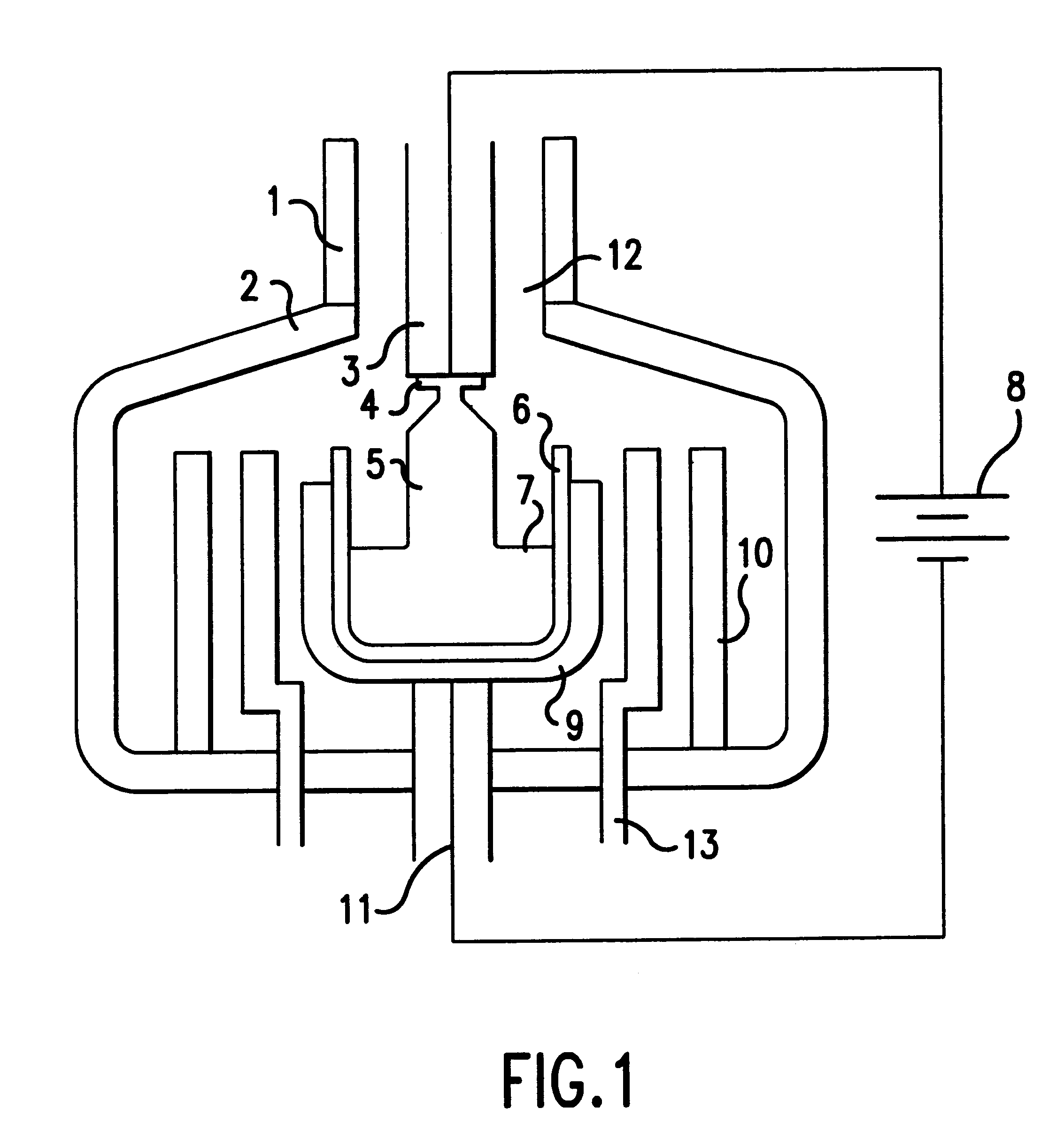
A power source is attached to a pulling member and a graphite susceptor holding a quartz crucible containing polycrystalline silicon as a raw material. A silicon crystal is grown from this raw material, is then re-melted, and then grown again.

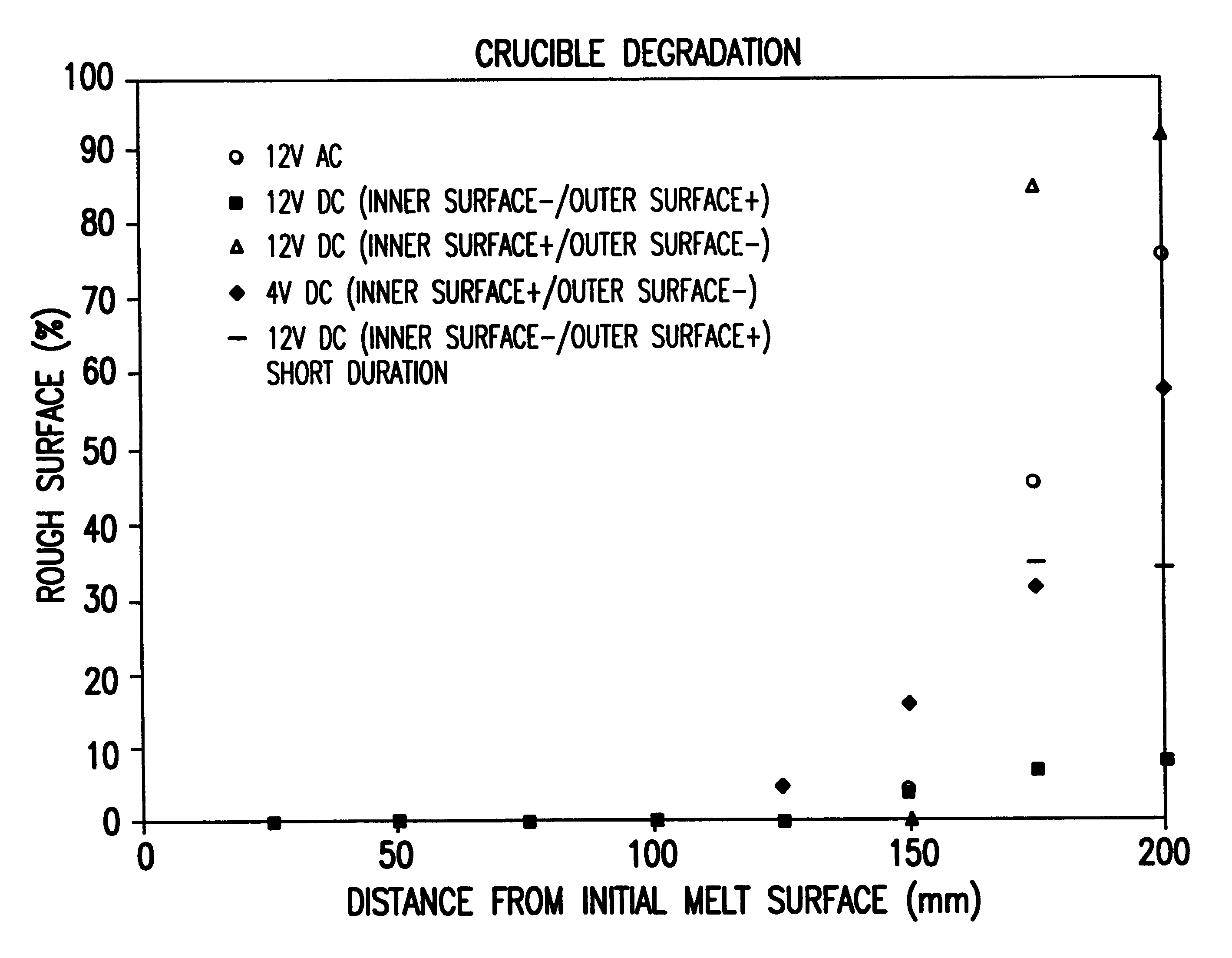
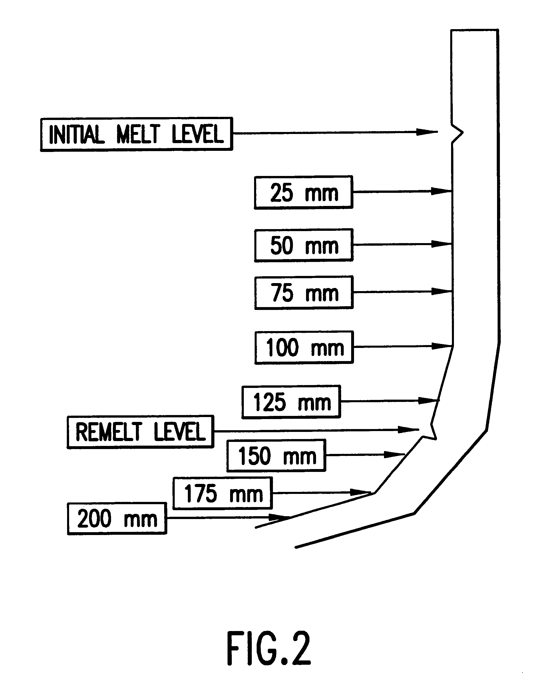
The crystal growing process is repeated several times, varying the voltage and / or the type or polarity of the power source. After each crystal growing operation, crucible degradation is visually measured. In particular, a ruler is used to measure the distance from the initial melt surface to the bottom of the crucible. (This is illustrated in FIG. 2.)

The resultant data is presented in the graph in FIG. 3. In FIG. 3, the measurements are graphed with respect to the rough surface % on the vertical axis, and the distance from the initial melt surface (mm) on the horizontal axis.

Based on this testing, it is found that the lowest degradation (rough surface=8%) is found using a 12 V DC power source with the negative terminal attached to the pulling m...


PUM

PropertyMeasurementUnit
electric potentialaaaaaaaaaa

Abstract

A method of manufacturing a crystal of silicon in accordance with a Czochralski method, includes the steps of applying an electric potential across a quartz crucible containing a silicon melt, and pulling a crystal of silicon from the silicon melt.

Description

1. Field of InventionThe present invention relates to a method of manufacturing a crystal of silicon through use of the Czochralski method (CZ method).2. Description of Related ArtWhen a crystal of silicon is pulled from silicon melt within a quartz crucible in accordance with the CZ method, the inner surface of the crucible is exposed to the silicon melt, which is maintained at a high temperature. As a result, the condition of the inner surface of the crucible changes and deteriorates. In particular, the vitreous silica changes to a crystalline form, .beta.-cristobalite. The phase change occurs at many nucleation sites on the inner surface of the crucible. As dissolution of the inner layer occurs, there is potential of undercutting of the .beta.-cristobalite formations. If the undercutting is severe enough, the formation may be released into the silicon melt. If the .beta.-cristobalite separates from the inner surface of the crucible and adheres to the surface of a crystal of silic...

Claims


Application Information

Patent Timeline
Patent Type & Authority Patents(United States)
IPC IPC(8): C30B15/10C30B15/00C30B29/06
CPCC30B15/10C30B29/06
Inventor BABA, MASAHIKOKIRKLAND, SCOTT MATTHEWRUDBERG, RICHARD WILLIAMSONOKAWA, SUSUMUTAIE, DARREN MARKUCHIKAWA, AKIRA
Owner SEH AMERICA
Why Eureka
Try Eureka