

Semiconductor device using positive photosensitive resin composition and process for preparation thereof
a technology of positive photosensitive resin and semiconductor device, which is applied in the direction of photosensitive material processing, photomechanical equipment, instruments, etc., can solve the problems of high sensitivity of photosensitive resin, long exposure time per one sheet of wafer, etc., and achieve excellent adhesion to encapsulating resin and substrate, high sensitivity, and high yield of residual film thickness
Inactive Publication Date: 2001-05-22
SUMITOMO BAKELITE CO LTD
View PDF28 Cites 25 Cited by
- Summary
- Abstract
- Description
- Claims
- Application Information
AI Technical Summary
Benefits of technology
An object of this invention is to provide a positive type photosensitive resin which has a high sensitivity and can give a pattern with a high yield of residual film thickness and is excellent in adhesion to an encapsulating resin and a substrate.
Another object of this invention is to provide a semiconductor device having a high reliability in which a pattern of a polybenzoxazole resin has been formed with a high yield of residual film thickness on a semiconductor element by using the above positive type photosensitive resin excellent in adhesion to an encapsulating resin.
The positive type photosensitive resin composition of this invention can have, if necessary, added thereto a dihydropyridine derivative for enhancing the photosensitive characteristics. The dihydropyridine derivative includes, for example, 2,6-dimethyl-3,5-diacetyl-4-(2'-nitrophenyl)-1,4-dihydropyridine, 4-(2'-nitrophenyl)-2,6-dimethyl-3,5-dicarboethoxy-1,4-dihydropyridine, 4-(2',4'-dinitrophenyl)-2,6-dimethyl-3,5-carbomethoxy-1,4-dihydropyridine and the like.
However, when the phenol compound represented by the general formula (2) or (3) of this invention is used, the dissolution rate in the exposed portion is increased, and the sensitivity is enhanced. Furthermore, the film loss in the unexposed portion as seen when the sensitivity is increased by reducing the molecular weight is very small. In this invention, moreover, by adding the phenol compound represented by the general formula (2) or (3), there can be obtained a positive type photosensitive resin composition having such new characteristics that the adhesion of the composition to an encapsulating resin is enhanced, and when this composition is coated on the surface of a semiconductor element, it has been confirmed that the reliability of the semiconductor device is enhanced.
The phenol compound represented by the general formula (2) is low in solubility at low temperatures, so that when, for example, a composition containing the phenol compound represented by the general formula (2) is stored at a very low temperature, the deposition of the phenol compound of the general formula (2) is seen in some cases. In such a case, a part of the phenol compound of the general formula (2) can be replaced by a phenol compound of the general formula (3) to enhance the storability at low temperatures.
Problems solved by technology
However, in the development step, a solvent such as N-methyl-2-pyrrolidone or the like becomes necessary, so that the use of the above polyimides has a problem in respects of safety and handling.
When such a photosensitive resin is actually used, the sensitivity of the photosensitive resin particularly becomes a problem.
When the sensitivity is low, the exposure time per one sheet of wafer becomes long, and the throughput becomes low.
Therefore, when, for example, the molecular weight of the polybenzoxazole resin as the base resin is made small for the purpose of enhancing the sensitivity of the photosensitive resin, there are caused such problems that the film loss of the unexposed portion during the development becomes large and the pattern shape becomes bad.
Moreover, the adhesion between the photosensitive resin and the encapsulating resin is bad, and delamination is caused at the interface therebetween, so that there is a problem in practical use.
However, the above photosensitive polybenzoxazole precursor is inferior in adhesion to a substrate, particularly a silicon wafer, and has such a serious problem that the resin is peeled from the substrate by a treatment at a high temperature at a high humidity after curing This problem cannot be completely solved by adding to the precursor a silane coupling agent or the like which is put on market for improving adhesion, and at present, the use thereof is severely limited.
Method used
View moreImage
Smart ImageViewing Examples

Examples
example 2
The same procedure as in Example 1 was repeated, except that the phenol compound (P-1) was replaced by a phenol compound represented by the structural formula (P-2): ##STR44##
to obtain the results shown in Table 1.
example 3
The same procedure as in Example 1 was repeated, except that the phenol compound (P-1) was replaced by a mixture of phenol compounds represented by the structural formulas (P-3): ##STR45##
to obtain the results shown in Table 1.
example 4
The same procedure as in Example 1 was repeated, except that the amount of the phenol compound (P-1) added was changed to 5 parts by weight, to obtain the results shown in Table 1.
Login to View More PUM
| Property | Measurement | Unit |
|---|---|---|
| thickness | aaaaa | aaaaa |
| tensile elongation | aaaaa | aaaaa |
| temperature | aaaaa | aaaaa |
Abstract
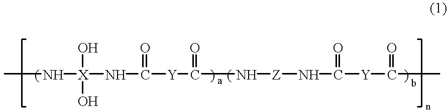
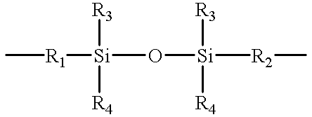
A positive type photosensitive resin composition which comprises (A) 100 parts by weight of a polyamide represented by the general formula (1):wherein X represents a tetravalent aromatic group; Y represents a divalent aromatic group; Z represents a divalent group represented by the formula:in which R1 and R2 represent divalent organic groups and R3 and R4 represent monovalent organic groups; a and b represent molar fractions; a+b=100 mole %; a=60.0-100.0 mole %; b=0-40.0 mole %; and n represents an integer of 2 to 500, (B) 1 to 100 parts by weight of a photosensitive diazoquinone compound and (C)1 to 50 parts by weight of a phenol compound represented by a specific structural formula and / or (D) 0.1 to 20 parts by weight of an organosilicon compound represented by a specific structural formula; and a semiconductor device in which a pattern of a polybenzoxazole resin obtained by using the above photosensitive resin composition is formed in a thickness of 0.1 to 20 mum on a semiconductor element.
Description
1. Field of the InventionThis invention relates to a positive type photosensitive resin composition which has a high sensitivity, can give a pattern with a high yield of residual film thickness and is excellent in adhesion to an encapsulating resin and a substrate, and to a semiconductor device provided with a film which is formed from the above positive type photosensitive resin composition and which relaxes the impact due to the working of molding a resin during encapsulating and also relaxes the stress caused in various thermal histories after the molding.2. Description of Related ArtPolyimide resins having excellent heat resistance, excellent electrical characteristics and excellent mechanical characteristics have heretofore been used for a surface-protecting film of a semiconductor element and an interlaminar insulation film of a semiconductor element. Recently, however, a remarkable enhancement of heat cycle resistance, thermal shock resistance and the like have been required ...
Claims
Login to View More Application Information
Patent Timeline
 Patent Type & AuthorityPatents(United States)
IPC IPC(8): G03F7/075G03F7/022
CPCG03F7/0226G03F7/0755G03F7/0757Y10S430/107G03F7/00G03F7/012
InventorHIRANO, TAKASHIBANBA, TOSHIOMAKABE, HIROAKITAKEDA, NAOSHIGETAKEDA, TOSHIRO
OwnerSUMITOMO BAKELITE CO LTD