Method for packaging a semiconductor chip

Inactive Publication Date: 2001-06-05
ADVANCED SEMICON ENG INC
View PDF3 Cites 29 Cited by
  • Summary
  • Abstract
  • Description
  • Claims
  • Application Information

AI Technical Summary

Benefits of technology

It should be noted here that after the step of encapsulating both the semiconductor chip 240 and the conducting wires 250 by the upper molding compound layer 260 as shown in FIG. 3G, a curing process is required to complete the encapsulated chip package. On the other hand, after the step of pre-molding the insulating sections 230 with a molding compound into the openings 220 as shown in FIG. 3D, the molding compound is cooled at room temperature without proceeding a curing process. As a result of not curing the molding compound of the insulating sections 230 during and after the step of pre-molding the insulating sections 230 such that the chemical binding among t

Problems solved by technology

However, the pin count of a package such as DIP (dual inline package) according to a conventional packaging method typically is not high enough.
Nonetheless, since the exposed leads 13 are not completely encapsulated by the molding material 12, the leads 13 can not be anchored securely by

Method used


Image

  • Method for packaging a semiconductor chip
  • Method for packaging a semiconductor chip
  • Method for packaging a semiconductor chip

Examples


Example

Example 2

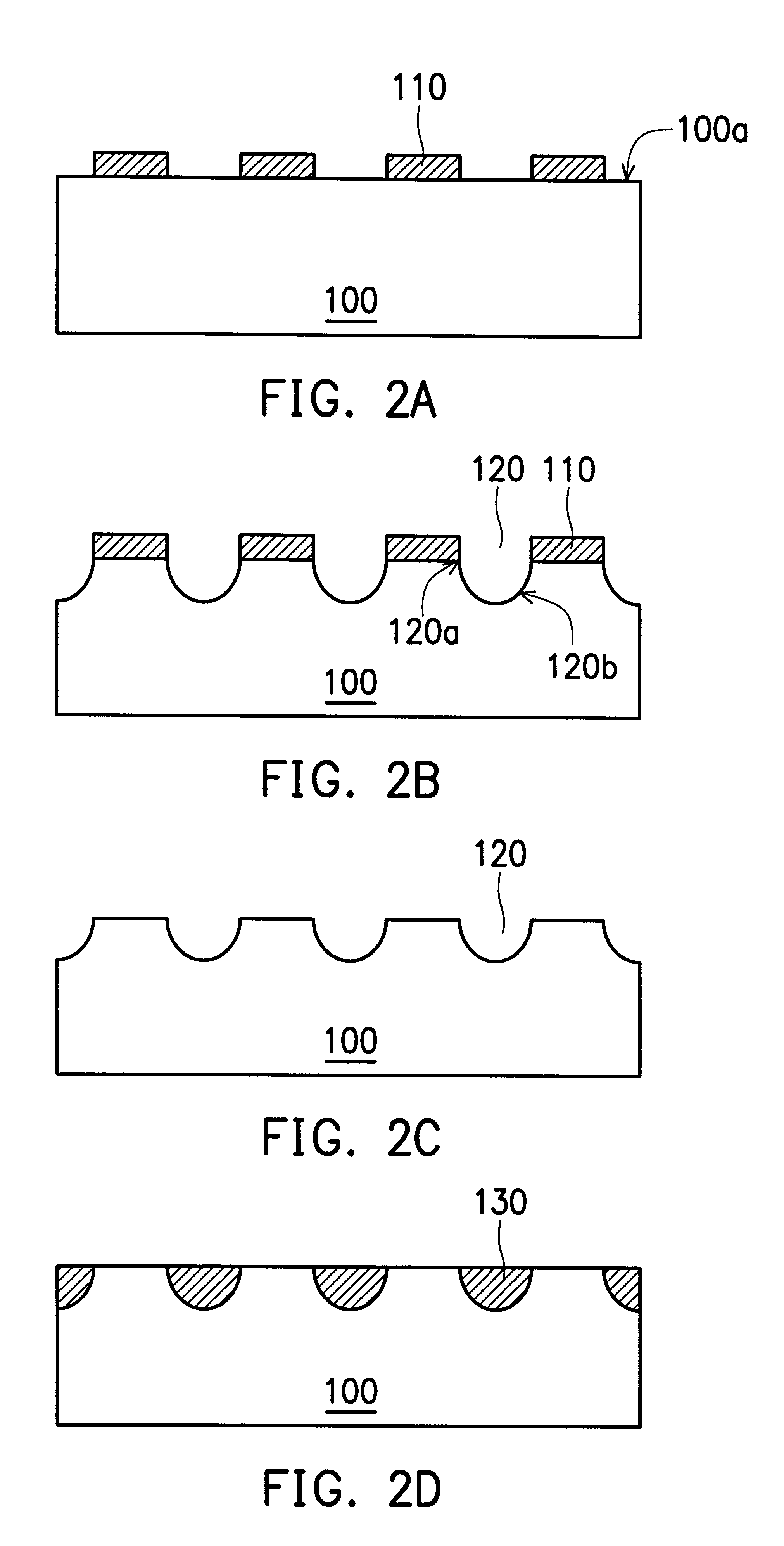
FIG. 3A through FIG. 3G schematically depict in cross-sectional views steps involved in a method for packaging a semiconductor chip according to a second example of the present invention.

Referring to FIG. 3A through FIG. 3C, whereas steps for forming a plurality of openings in the lead region are shown with the upper portions of the openings formed larger than the lower portions of the openings. For example, referring to FIG. 3A, a conducting substrate 200 made of copper is provided with a lead region and a chip region. Then a photoresist layer 210 is coated and patterned on the top surface 200a of the conducting substrate 200. Subsequently, referring to FIG. 3B, using the patterned photoresist layer 210 as a mask, the top surface of the conducting substrate 200 is then etched to form a plurality of openings 220 in the lead region 220', wherein the etching process can be either a wet etching or dry etching process. It should be noted here that the upper portions 220a of the...


PUM


Abstract

A method for packaging a semiconductor chip, generally comprising the following steps of: (a) forming a plurality of openings on the top surface of the conducting substrate, wherein the upper portions of the openings are formed larger than the lower portions of the openings; (b) forming insulating sections in the conducting substrate by filling an insulating material in the openings; (c) forming a plurality of leads insulated by the insulating sections by planarizing the bottom surface of the conducting substrate to expose and form planarized bottom surfaces of the insulating sections; (d) mounting a semiconductor chip on the bottom surface of the conducting substrate; (e) providing a plurality of conducting wires to electrically connect the semiconductor chip to the leads; and (f) encapsulating the semiconductor chip and the conducting wires. The package according to the present invention is characterized by upper portions of the leads that are purposedly formed larger than lower portions of the leads which prevents the leads from being easily detachable and the package from being destructed by water, the reliability of the package is thus increased.

Description

1. Field of the InventionThe present invention relates to a method for packaging a semiconductor chip; more particularly, the present invention relates to a method for packaging a semiconductor that generally forms larger upper portions of the leads relative to lower portions of the leads.2. Description of the Prior ArtMicroelectronic devices are typically comprised of one or more silicon die having, at least in part of, a multitude of die bond pads on a front surface, a chip body, and an interconnection scheme to connect the pads on the die to a supporting substrate and an encapsulating to ensure that the die is protected from contaminants. The combination of these elements is generally referred to as a chip package.However, the pin count of a package such as DIP (dual inline package) according to a conventional packaging method typically is not high enough. Thus, the latest trend has been emphasized on a BGA (ball grid array) package as shown in FIG. 1, which is developed to addre...

Claims


Application Information

Patent Timeline
IPC IPC(8): H01L21/48H01L23/28H01L21/67H01L23/31H01L23/498H01L21/02H01L23/48H01L21/68
CPCH01L21/486H01L21/6835H01L23/3107H01L23/3128H01L23/49827H01L2221/68377H01L2224/48091H01L2924/00014H01L24/48H01L2224/73265H01L2924/10253H01L2924/00H01L2224/05599H01L2224/85399H01L2924/181H01L2924/18165H01L2224/45099H01L2924/00012H01L2224/45015H01L2924/207
Inventor KANG, KUN-AJUNG, KYUJINPARK, HYUNG JUNLEE, JUN HONG
Owner ADVANCED SEMICON ENG INC
Why Eureka
Try Eureka